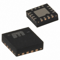
SY89875UMG Micrel Inc, SY89875UMG Datasheet - Page 5

SY89875UMG
Manufacturer Part Number
SY89875UMG
Description
IC CLK DIVIDER/1:2 BUFFER 16-MLF
Manufacturer
Micrel Inc
Type
Fanout Buffer (Distribution), Dividerr
Series
Precision Edge®r
Datasheet
1.SY89875UMG.pdf
(10 pages)
Specifications of SY89875UMG
Number Of Circuits
1
Ratio - Input:output
1:2
Differential - Input:output
Yes/Yes
Input
CML, HSTL, LVDS, LVPECL
Output
LVDS
Frequency - Max
2.5GHz
Voltage - Supply
2.375 V ~ 2.625 V
Operating Temperature
-40°C ~ 85°C
Mounting Type
Surface Mount
Package / Case
16-MLF®, QFN
Frequency-max
2.5GHz
Number Of Clock Inputs
1
Mode Of Operation
Differential
Output Frequency
>2000MHz
Output Logic Level
LVDS
Operating Supply Voltage (min)
2.375V
Operating Supply Voltage (typ)
2.5V
Operating Supply Voltage (max)
2.625V
Package Type
MLF
Operating Temp Range
-40C to 85C
Operating Temperature Classification
Industrial
Mounting
Surface Mount
Pin Count
16
Lead Free Status / RoHS Status
Lead free / RoHS Compliant
Other names
576-2105-5
SY89875UMG
SY89875UMG
Available stocks
Company
Part Number
Manufacturer
Quantity
Price
Company:
Part Number:
SY89875UMG
Manufacturer:
MICREL
Quantity:
30
Part Number:
SY89875UMGTR
Manufacturer:
MICREL/麦瑞
Quantity:
20 000
V
Symbol
f
t
t
t
t
t
Note 1.
Note 2.
Note 3.
Note 4.
Note 5.
Note 6.
M9999-082407
hbwhelp@micrel.com or (408) 955-1690
Micrel, Inc.
MAX
PD
SKEW
RR
JITTER
r
,t
CC
AC ELECTRICAL CHARACTERISTICS
f
TIMING DIAGRAM
= 2.5V ±5%; T
Measured with 400mV input signal, 50% duty cycle, all outputs loaded with 100ý across each output pair, unless otherwise stated.
Specification for packaged product only.
Skew is measured between outputs under identical transitions.
See “Timing Diagram.”
Cycle-to-cycle jitter definition: the variation in period between adjacent cycles over a random sample of adjacent cycle pairs. T
where T is the time between rising edges of the output signal.
Total jitter definition: with an ideal clock input of frequency - f
the specified peak-to-peak jitter value.
Parameter
Maximum Input Frequency
Differential Propagation Delay
IN to Q
Within-Device Skew (diff.)
Part-to-Part Skew (diff.)
Reset Recovery Time
Cycle-to-Cycle Jitter
Total Jitter
Rise/Fall Time (20% to 80%)
A
= –40°C to +85°C; Unless otherwise stated.
/RESET
/IN
/Q
IN
Q
V
IN
V
Swing
ID
Condition
Output Swing ž 200mV
Input Swing < 400mV
Input Swing ž 400mV
Note 3
Note 3
Note 4
Note 5
Note 6
(Notes 1, 2)
MAX
, no more than one output edge in 10
5
V
t
CC/2
RR
t
PD
V
OUT
12
Min
590
540
600
output edges will deviate by more than
2.0
Swing
70
Typ
690
690
120
2.5
5
Precision Edge
Max
820
280
870
200
15
10
jitter_cc
1
SY89875U
= T
ps
Units
n
ps
GHz
–T
ps
ps
ps
ps
ps
ps
RMS
PP
n+1
®
,


