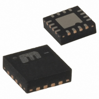
SY89875UMG Micrel Inc, SY89875UMG Datasheet - Page 2

SY89875UMG
Manufacturer Part Number
SY89875UMG
Description
IC CLK DIVIDER/1:2 BUFFER 16-MLF
Manufacturer
Micrel Inc
Type
Fanout Buffer (Distribution), Dividerr
Series
Precision Edge®r
Datasheet
1.SY89875UMG.pdf
(10 pages)
Specifications of SY89875UMG
Number Of Circuits
1
Ratio - Input:output
1:2
Differential - Input:output
Yes/Yes
Input
CML, HSTL, LVDS, LVPECL
Output
LVDS
Frequency - Max
2.5GHz
Voltage - Supply
2.375 V ~ 2.625 V
Operating Temperature
-40°C ~ 85°C
Mounting Type
Surface Mount
Package / Case
16-MLF®, QFN
Frequency-max
2.5GHz
Number Of Clock Inputs
1
Mode Of Operation
Differential
Output Frequency
>2000MHz
Output Logic Level
LVDS
Operating Supply Voltage (min)
2.375V
Operating Supply Voltage (typ)
2.5V
Operating Supply Voltage (max)
2.625V
Package Type
MLF
Operating Temp Range
-40C to 85C
Operating Temperature Classification
Industrial
Mounting
Surface Mount
Pin Count
16
Lead Free Status / RoHS Status
Lead free / RoHS Compliant
Other names
576-2105-5
SY89875UMG
SY89875UMG
Available stocks
Company
Part Number
Manufacturer
Quantity
Price
Company:
Part Number:
SY89875UMG
Manufacturer:
MICREL
Quantity:
30
Part Number:
SY89875UMGTR
Manufacturer:
MICREL/麦瑞
Quantity:
20 000
Micrel, Inc.
Note 1.
M9999-082407
hbwhelp@micrel.com or (408) 955-1690
/RESET
PACKAGE/ORDERING INFORMATION
TRUTH TABLE
Pin Number
PIN DESCRIPTION
/Q0
/Q1
0
Q0
Q1
1, 2, 3, 4
16, 15, 5
1
1
1
1
1
(1)
12, 9
7, 14
10
11
13
6
8
(1)
Reset/Disable function is asserted on the next clock input
(IN, /IN) high-to-low transition.
16-Pin MLF
1
2
3
4
16
S2
5
X
0
1
1
1
1
15
6
S1
14
7
X
X
0
0
1
1
S0, S1, S2
Pin Name
/DISABLE
VREF-AC
/RESET,
Exposed
®
Q0, /Q0
Q1, /Q1
IN, /IN
GND
13
VCC
8
(MLF-16)
NC
VT
S0
12
11
X
X
10
0
1
0
1
9
IN
VT
VREF-AC
/IN
Outputs
Reference Clock (pass through)
Reference Clock ÷2
Reference Clock ÷4
Reference Clock ÷8
Reference Clock ÷16
Q = LOW, /Q = HIGH
Clock Disable
Pin Function
Differential Input: Internal 50ý termination resistors to V
differential input. See “Input Interface Applications” section.
Differential Buffered LVDS Outputs: Divided by 1, 2, 4, 8 or 16. See “Truth Table.”
Select Pins: See “Truth Table.” LVTTL/CMOS logic levels. Internal 25ký pull-up resistor.
Logic HIGH if left unconnected (divided by 16 mode.) Input threshold is V
No Connect.
LVTTL/CMOS Logic Levels: Internal 25ký pull-up resistor. Logic HIGH if left unconnected.
Apply LOW to reset the divider (divided by 2, 4, 8 or 16 mode). Also acts as a disable/enable
function. The reset and disable function occurs on the next high-to-low clock input transition.
Input threshold is V
Reference Voltage: Equal to V
Decouple the V
Termination Center-Tap: For CML or LVDS inputs, leave this pin floating. Otherwise, See
Figures 4a to 4f, “Input Interface Applications” section.
Positive Power Supply: Bypass with 0.1µF//0.01µF low ESR capacitor.
Ground. Exposed pad must be connected to the same potential as the GND pin.
Unused output pairs must be terminated with 100ý across the different pair.
Ordering Information(1)
Notes:
1. Contact factory for die availability. Dice are guaranteed at T
2. Tape and Reel.
3. Pb-Free package is recommended for new designs.
Part Number
SY89875UMI
SY89875UMITR
SY89875UMG
SY89875UMGTR
REF–AC
CC
/2.
pin with a 0.01µF capacitor. See “Input Interface Applications” section.
(3)
(2)
(2, 3)
2
CC
–1.4V (approx.). Used for AC-coupled applications only.
Package Operating
MLF-16
MLF-16
MLF-16
MLF-16
Type
Industrial
Industrial
Industrial
Industrial
Range
T
input. Flexible input accepts any
Pb-Free bar line indicator
Pb-Free bar line indicator
A
= 25°C, DC Electricals only.
875U with
875U with
Package
Marking
875U
875U
CC
/2.
Precision Edge
SY89875U
Pb-Free
Pb-Free
NiPdAu
NiPdAu
Finish
Sn-Pb
Sn-Pb
Lead
®


