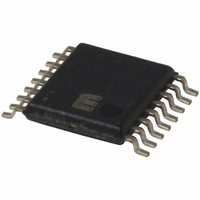
SY100EP15VK4G Micrel Inc, SY100EP15VK4G Datasheet - Page 8

SY100EP15VK4G
Manufacturer Part Number
SY100EP15VK4G
Description
IC BUFFER FAN 1:4 3.3/5V 16TSSOP
Manufacturer
Micrel Inc
Type
Fanout Buffer (Distribution), Multiplexerr
Series
100EP, Precision Edge®, ECL Pro™r
Datasheet
1.SY100EP15VK4G.pdf
(9 pages)
Specifications of SY100EP15VK4G
Number Of Circuits
1
Ratio - Input:output
4:4
Differential - Input:output
Yes/Yes
Input
HSTL, LVECL, LVPECL
Output
LVECL, LVPECL
Frequency - Max
2.5GHz
Voltage - Supply
2.97 V ~ 5.5 V
Operating Temperature
-40°C ~ 85°C
Mounting Type
Surface Mount
Package / Case
16-TSSOP
Frequency-max
2.5GHz
Frequency
2.5GHz
No. Of Outputs
4
Supply Current
52mA
Supply Voltage Range
± 2.97V To ± 3.63V, ± 4.5V To ± 5.5V
Digital Ic Case Style
TSSOP
No. Of Pins
16
Number Of Clock Inputs
2
Operating Supply Voltage (min)
-2.97/2.97V
Operating Supply Voltage (typ)
-3.3/-5/3.3/5V
Operating Supply Voltage (max)
-5.5/5.5V
Package Type
TSSOP
Operating Temp Range
-40C to 85C
Operating Temperature Classification
Industrial
Mounting
Surface Mount
Pin Count
16
Lead Free Status / RoHS Status
Lead free / RoHS Compliant
Other names
576-1992-5
SY100EP15VK4G
SY100EP15VK4G
Available stocks
Company
Part Number
Manufacturer
Quantity
Price
Company:
Part Number:
SY100EP15VK4G
Manufacturer:
MICREL
Quantity:
2 050
Micrel, Inc.
Notes:
1. For +2.5V systems: R1 = 250Ω, R2 = 62.5Ω.
2. For +5.0V systems: R1 = 82Ω, R2 = 130Ω.
Notes:
1. Power-saving alternative to Thevenin termination.
2. Place termination resistors as close to destination inputs as possible.
3. R
4. C1 is an optional bypass capacitor intended to compensate for any tr/tf mismatches.
Notes
1. Unused output (/Q) must be terminated to balance the output.
2. Micrel’s differential I/O logic devices include a V
3. Connect unused input through 50Ω to V
4. For +2.5V systems: R1 = 250Ω, R2 = 62.5Ω.
M9999-120505
hbwhelp@micrel.com or (408) 955-1690
TERMINATION RECOMMENDATIONS
b
resistor sets the DC bias voltage, equal to V
Figure 1. Parallel Termination–Thevenin Equivalent
BB
+3.3V
+3.3V
. Bypass with a 0.01µF capacitor to V
“source”
Figure 2. Three-Resistor “Y–Termination”
T
/Q
Q
BB
+3.3V
. For +3.3V systems R
+3.3V
Figure 3. Terminating Unused I/O
reference pin .
R1
130Ω
R2
82Ω
V
Z
Z
t
= V
O
O
= 50Ω
= 50Ω
Z
CC
Z = 50Ω
Z = 50Ω
O
= 50Ω
–2V
R1
130Ω
R2
82Ω
b
50Ω
8
50Ω
= 46Ω to 50Ω. For +5V systems, R
+3.3V
+3.3V
R1
130Ω
R2
82Ω
CC
R
50Ω
b
, not GND.
R1
130Ω
R2
82Ω
+3.3V
“destination”
(Optional)
C1
0.01µF
50Ω
0.01µF
+3.3V
V
+3.3V
t
+3.3V
= V
CC
V
BB
–2V
b
= 110Ω.
SY100EP15V
ECL Pro™


