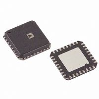
AD9513BCPZ Analog Devices Inc, AD9513BCPZ Datasheet - Page 9

AD9513BCPZ
Manufacturer Part Number
AD9513BCPZ
Description
IC CLOCK DIST 3OUT PLL 32LFCSP
Manufacturer
Analog Devices Inc
Type
Fanout Buffer (Distribution), Dividerr
Datasheet
1.AD9513BCPZ.pdf
(28 pages)
Specifications of AD9513BCPZ
Number Of Circuits
1
Ratio - Input:output
1:3
Differential - Input:output
Yes/Yes
Input
Differential
Output
CMOS, LVDS
Frequency - Max
800MHz
Voltage - Supply
3.135 V ~ 3.465 V
Operating Temperature
-40°C ~ 85°C
Mounting Type
Surface Mount
Package / Case
32-LFCSP
Frequency-max
800MHz
No. Of Multipliers / Dividers
3
No. Of Amplifiers
4
Supply Voltage Range
3.135V To 3.465V
Slew Rate
1V/ns
Operating Temperature Range
-40°C To +85°C
Digital Ic Case Style
LFCSP
Package
32LFCSP EP
Lead Free Status / RoHS Status
Lead free / RoHS Compliant
For Use With
AD9513/PCBZ - BOARD EVAL CLOCK 3CH AD9513
Lead Free Status / RoHS Status
Lead free / RoHS Compliant, Lead free / RoHS Compliant
Available stocks
Company
Part Number
Manufacturer
Quantity
Price
Company:
Part Number:
AD9513BCPZ
Manufacturer:
ADI
Quantity:
3 000
Company:
Part Number:
AD9513BCPZ
Manufacturer:
ADI
Quantity:
140
Company:
Part Number:
AD9513BCPZ-REEL7
Manufacturer:
AD
Quantity:
1 000
Company:
Part Number:
AD9513BCPZ-REEL7
Manufacturer:
ADI
Quantity:
3 000
Part Number:
AD9513BCPZ-REEL7
Manufacturer:
ADI/亚德诺
Quantity:
20 000
Parameter
DELAY BLOCK ADDITIVE TIME JITTER
1
SYNCB, VREF, AND SETUP PINS
Table 6.
Parameter
SYNCB
VREF
S0 TO S10
POWER
Table 7.
Parameter
POWER-ON SYNCHRONIZATION
POWER DISSIPATION
POWER DELTA
1
This value is incremental. That is, it is in addition to the jitter of the LVDS or CMOS output without the delay. To estimate the total jitter, the LVDS or CMOS output jitter
should be added to this value using the root sum of the squares (RSS) method.
This is the rise time of the V
transition the range from 2.2 V to 3 .1 V. If the rise time is too slow, the outputs are not synchronized.
Delay FS = 1.8 ns Fine Adj. 00000
Delay FS = 1.8 ns Fine Adj. 11111
Delay FS = 6.0 ns Fine Adj. 00000
Delay FS = 6.0 ns Fine Adj. 11111
Delay FS = 11.6 ns Fine Adj. 00000
Delay FS = 11.6 ns Fine Adj. 11111
Logic High
Logic Low
Capacitance
Output Voltage
Levels
V
Divider (Divide = 2 to Divide = 1)
LVDS Output
CMOS Output (Static)
CMOS Output (@ 62.5 MHz)
CMOS Output (@ 125 MHz)
Delay Block
S
Transit Time from 2.2 V to 3.1 V
0
1/3
2/3
1
S
supply that is required to ensure that a synchronization of the outputs occurs on power-up. The critical factor is the time it takes the V
Min
2.7
0.62·V
0.2·V
0.55·V
0.9·V
1
S
S
S
S
1
Min
175
240
320
15
20
30
65
70
30
Typ
2
40
110
145
Typ
325
460
605
30
50
45
Max
0.40
0.76·V
0.1·V
0.45·V
0.8·V
Min
Max
35
575
615
840
45
85
50
155
220
65
S
S
S
S
Typ
0.71
1.2
1.3
2.7
2.0
2.8
Rev. 0 | Page 9 of 28
Unit
ms
mW
mW
mW
mW
mW
mW
mW
mW
mW
Unit
V
V
pF
V
V
V
V
V
Max
Single-ended. At 62.5 MHz out with 5 pF load.
Single-ended. At 125 MHz out with 5 pF load.
Test Conditions/Comments
See the Power-On SYNC section.
All three outputs on. LVDS (divide = 2). No clock. Does not include
power dissipated in external resistors.
All three outputs on. CMOS (divide = 2); 62.5 MHz out (5 pF load).
All three outputs on. CMOS (divide = 2); 125 MHz out (5 pF load).
For each divider. No clock.
No clock.
No clock.
Off to 1.8 ns fs, delay word = 60; output clocking at 62.5 MHz.
Test Conditions/Comments
Minimum − maximum from 0 mA to 1 mA load
Unit
ps rms
ps rms
ps rms
ps rms
ps rms
ps rms
Test Conditions/Comments
100 MHz output; incremental additive jitter
AD9513
1
S
to


