EL5001IL-T7 Intersil, EL5001IL-T7 Datasheet - Page 8
EL5001IL-T7
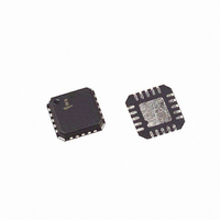
Manufacturer Part Number
EL5001IL-T7
Description
IC CLOCK DRIVER 6-CHAN 20-QFN
Manufacturer
Intersil
Type
Buffer/Driverr
Datasheet
1.EL5001ILZ-T13.pdf
(8 pages)
Specifications of EL5001IL-T7
Input
CMOS, TTL
Operating Temperature
-40°C ~ 85°C
Mounting Type
Surface Mount
Package / Case
20-VQFN Exposed Pad, 20-HVQFN, 20-SQFN, 20-DHVQFN
Lead Free Status / RoHS Status
Contains lead / RoHS non-compliant
Voltage - Supply
-
Frequency-max
-
Output
-


Applications Information
The EL5001, a six channel high performance buffer, is
directed primarily as a clock driver to LPTS LCD display
applications. The six input channels are grouped into one
group of four inputs and one group of two inputs each with a
single pin (INV1 or INV2) to toggle the polarity from inverting
to non-inverting. Each channel consists of a single N-
channel low side driver and single P-channel high side
driver. These 11Ω devices pull the output to either the high or
low voltage on V
logic input signal.
A common 3-state pin is available that when activated will
pull all 6-channel outputs to the high impedance state.
Enable and disable pins turn shutdown both inputs and
outputs. Timing plots for 3-state, enable, and disable
functions are included in the characterization
documentation.
The EL5001 is available in either a 20-pin HTSSOP or QFN
(4mm x 4mm) packages to provide a choice for power
dissipation considerations.
Supply Voltage and Input Compatibility
The EL5001 is designed to operate at a maximum potential
range from 0V to 18V. Because the EL5001 does not contain
a true analog switch, the positive supply must always be 4V
higher than the negative supply.
All input pins are compatible with both 3V and 5V CMOS
signals. With the positive supply set to V
is compatible with TTL inputs.
Power Supply Bypassing
Due to the high switching currents generated by the EL5001
power supply bypassing is very important on both the
positive and negative supplies. A 4.7µF tantalum capacitor
can be used in parallel with a 0.1µF low-inductance ceramic
MLC capacitor. As with all bypass components, these should
be placed as close as possible to the supply pins. We also
recommend the V
bypassing especially when the device is driving highly
capacitive loads.
Intersil products are sold by description only. Intersil Corporation reserves the right to make changes in circuit design, software and/or specifications at any time without
notice. Accordingly, the reader is cautioned to verify that data sheets are current before placing orders. Information furnished by Intersil is believed to be accurate and
reliable. However, no responsibility is assumed by Intersil or its subsidiaries for its use; nor for any infringements of patents or other rights of third parties which may result
from its use. No license is granted by implication or otherwise under any patent or patent rights of Intersil or its subsidiaries.
All Intersil U.S. products are manufactured, assembled and tested utilizing ISO9000 quality systems.
H
L
and V
and V
Intersil Corporation’s quality certifications can be viewed at www.intersil.com/design/quality
For information regarding Intersil Corporation and its products, see www.intersil.com
L
H
respectively, depending on the
pins have some level of
8
S
= 5V the EL5001
EL5001
Power Dissipation Calculation
When switching at high speeds, or driving heavy loads, the
EL5001 drive capability is limited by the rise in die
temperature brought about by internal power dissipation. For
reliable operation die temperature must be kept below
T
dissipation for a given application prior to selecting package
type.
Power dissipation may be calculated:
PD
where:
Having obtained the application's power dissipation, the
maximum junction temperature can be calculated:
T
where:
JMAX
JMAX
V
V
C
C
I
f = Frequency
T
T
PD = Power dissipation calculated above
θ
application (package + PCB combination)
S
JA
S
OUT
JMAX
MAX
L
INT
=
= Quiescent supply current (3mA max)
= Load capacitance
= Total power supply to the EL5001 (from V
(
= Thermal resistance, junction to ambient, of the
V
(125°C). It is necessary to calculate the power
=
= Internal load capacitance (80pF max)
S
= Swing on the output (V
= Maximum ambient operating temperature
T
= Maximum junction temperature (125°C)
×
MAX
I
S
)
+
+
4
Σ
1
Θ
×
JA
(
C
×
INT
PD
×
V
S
2
×
f )
H
+
- V
(
C
L
L
)
×
V
OUT
2
January 31, 2005
S
×
+ to V
f )
FN7376.2
S
-)
Related parts for EL5001IL-T7
Image
Part Number
Description
Manufacturer
Datasheet
Request
R

Part Number:
Description:
6-channel Clock Driver
Manufacturer:
Intersil Corporation
Datasheet:
Part Number:
Description:
Intersil Corporation [CMOS Serial Controller Interface]
Manufacturer:
Intersil Corporation
Datasheet:
Part Number:
Description:
Manufacturer:
Intersil Corporation
Datasheet:
Part Number:
Description:
357-036-542-201 CARDEDGE 36POS DL .156 BLK LOPRO
Manufacturer:
Intersil Corporation
Datasheet:
Part Number:
Description:
1024-Word x 4-Bit LSI Static RAM
Manufacturer:
Intersil Corporation
Datasheet:
Part Number:
Description:
General Purpose NPN Transistor Arrays FN341.4
Manufacturer:
Intersil Corporation
Datasheet:
Part Number:
Description:
CMOS 16-Bit Microprocessor
Manufacturer:
Intersil Corporation
Datasheet:
Part Number:
Description:
Manufacturer:
Intersil Corporation
Datasheet:
Part Number:
Description:
Manufacturer:
Intersil Corporation
Datasheet:
Part Number:
Description:
Manufacturer:
Intersil Corporation
Datasheet:
Part Number:
Description:
Manufacturer:
Intersil Corporation
Datasheet:
Part Number:
Description:
CMOS 6-Bit Latch and Decoder Memory Interfaces
Manufacturer:
Intersil Corporation
Datasheet:
Part Number:
Description:
CA3046General Purpose NPN Transistor Arrays
Manufacturer:
Intersil Corporation
Datasheet:
Part Number:
Description:
Manufacturer:
Intersil Corporation
Datasheet:
Part Number:
Description:
TR909 DLC/FLC SLIC with Low Power Standby
Manufacturer:
Intersil Corporation
Datasheet: