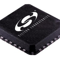
SI5023-D-GM Silicon Laboratories Inc, SI5023-D-GM Datasheet - Page 18

SI5023-D-GM
Manufacturer Part Number
SI5023-D-GM
Description
IC CLOCK/DATA RECVRY W/AMP 28MLP
Manufacturer
Silicon Laboratories Inc
Type
Clock and Data Recovery (CDR)r
Datasheet
1.SI5023-D-GM.pdf
(28 pages)
Specifications of SI5023-D-GM
Input
Differential
Output
CML
Frequency - Max
2.7GHz
Voltage - Supply
3.135 V ~ 3.465 V
Operating Temperature
-40°C ~ 85°C
Mounting Type
Surface Mount
Package / Case
28-VQFN Exposed Pad, 28-HVQFN, 28-SQFN, 28-DHVQFN
Frequency-max
2.7GHz
Lead Free Status / RoHS Status
Lead free / RoHS Compliant
Other names
336-1276
Si5023
4.11.2. Jitter Transfer
The
specifications related to SONET/SDH jitter transfer.
Jitter transfer is defined as the ratio of output signal jitter
to input signal jitter as a function of jitter frequency. (See
Figure 15.) These measurements are made with an
input test signal that is degraded with sinusoidal jitter
whose magnitude is defined by the mask in Figure 15.
4.11.3. Jitter Generation
The Si5023 exceeds all relevant specifications for jitter
generation proposed for SONET/SDH equipment. The
jitter generation specification defines the amount of jitter
that may be present on the recovered clock and data
outputs when a jitter free input signal is provided. The
18
Jitter (UI
Sinusoidal
Transfer
Figure 14. Jitter Tolerance Specification
Input
Figure 15. Jitter Transfer Specification
Jitter
0.1 dB
Si5023
SONET
Data Rate
OC-48
OC-12
OC-3
0.15
1.5
PP
15
)
exceeds
f0
10
10
10
F0
(Hz)
Acceptable
Range
SONET
Data Rate
OC-48
OC-12
OC-3
f1
600
30
30
F1
(Hz)
Frequency
all
Frequency
f2
F2
(kHz)
6000
300
300
relevant
Fc
2000
500
130
Slope = 20 dB/Decade
Fc
(kHz)
f3
F3
(kHz)
100
25
6.5
20 dB/Decade
ft
Slope
Bellcore/ITU
Ft
(kHz)
65
1000
250
Rev. 1.3
Si5023 typically generates less than 3.0 mUI
when presented with jitter-free input data.
4.12. RESET/DSPLL Calibration
The Si5023 achieves optimal jitter performance by
automatically calibrating the loop gain parameters within
the DSPLL on powerup. Calibration may also be
initiated by a high-to-low transition on the RESET/CAL
pin. The RESET/CAL pin must be held high for at least
1 µs. When RESET/CAL is released (set to low) the
digital logic resets to a known initial condition,
recalibrates the DSPLL, and will begin to lock to the
incoming data stream. For a valid reset to occur when
using Reference mode, a proper external reference
clock frequency must be applied as specified in Table 8.
4.13. Clock Disable
The Si5023 provides a clock disable pin (CLK_DSBL)
that is used to disable the recovered clock output
(CLKOUT). When the CLK_DSBL pin is asserted, the
positive and negative terminals of CLKOUT are tied to
VDD through 100 Ω on-chip resistors.
4.14. Data Squelch
The Si5023 provides a data squelching pin (DSQLCH)
that is used to set the recovered data output (DOUT) to
binary zero. When the DSQLCH pin is asserted, the
DOUT+ signal is held low (DOUT+ = 0) and the DOUT–
signal is held high (DOUT– = 1). This pin can be is used
to squelch corrupt data during LOS and LOL situations.
Care must be taken when ac coupling these outputs; a
long string of zeros or ones will not be held through ac
coupling capacitors.
4.15. Device Grounding
The Si5023 uses the GND pad on the bottom of the 28-
lead micro leaded package (QFN) for device ground.
This pad should be connected directly to the analog
supply ground. See Figure 21 on page 22 and Figure 22
on page 26 for the ground (GND) pad size and location.
4.16. Bias Generation Circuitry
The Si5023 makes use of an external resistor to set
internal bias currents. The external resistor allows
precise generation of bias currents, which significantly
reduces
implementations that use an internal resistor. The bias
generation circuitry requires a 10 kΩ (1%) resistor
connected between REXT and GND.
power
consumption
versus
rms
traditional
of jitter


