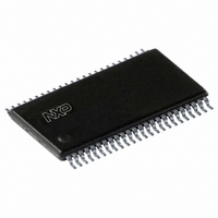
PCKV857ADGV,112 NXP Semiconductors, PCKV857ADGV,112 Datasheet - Page 4

PCKV857ADGV,112
Manufacturer Part Number
PCKV857ADGV,112
Description
IC 1:10 2.5V PLL CLK-DRVR48TSSOP
Manufacturer
NXP Semiconductors
Type
PLL Clock Driverr
Datasheet
1.PCKV857ADGG512.pdf
(13 pages)
Specifications of PCKV857ADGV,112
Input
SSTL-2
Output
SSTL-2
Frequency - Max
250MHz
Voltage - Supply
2.375 V ~ 2.625 V
Operating Temperature
0°C ~ 70°C
Mounting Type
Surface Mount
Package / Case
48-TVSOP
Frequency-max
250MHz
Lead Free Status / RoHS Status
Lead free / RoHS Compliant
Other names
935272776112
PCKV857ADGV
PCKV857ADGV
PCKV857ADGV
PCKV857ADGV
Philips Semiconductors
ABSOLUTE MAXIMUM RATINGS
NOTES:
1. Stresses beyond those listed under “absolute maximum ratings” may cause permanent damage to the device. These are stress ratings
2. The input and output negative voltage ratings may be exceeded if the input and output clamp-current ratings are observed.
3. This value is limited to 3.6 V maximum.
RECOMMENDED OPERATING CONDITIONS
NOTES:
1. Unused inputs must be held HIGH or LOW to prevent them from floating.
2. DC input signal voltage specifies the allowable DC execution of differential input.
3. Differential input signal voltage specifies the differential voltage |VTR - VCP| required for switching, where VTR is the true input level and
4. Differential cross-point voltage is expected to track variations of V
2003 Jul 31
SYMBOL
SYMBOL
100-250 MHz differential 1:10 clock driver
V
AV
only, and functional operation of the device at these or any other conditions beyond those indicated under “recommended operating
conditions” is not implied. Exposure to absolute-maximum-rated conditions for extended periods may affect device reliability.
VCP is the complementary input level.
T
V
V
AV
V
V
V
V
I
V
V
I
SR
DDQ
amb
T
OH
OL
I
V
OX
DDQ
I
OK
I
V
IH
ID
IX
DD
IL
IK
stg
O
DD
O
I
Supply voltage range
Supply voltage range
LOW-level input voltage
LOW-level input voltage
HIGH-level input voltage
HIGH-level input voltage
DC input signal voltage
DC differential input signal voltage
AC differential input signal voltage
Output differential cross-voltage
Input differential cross-voltage
HIGH-level output current
LOW-level output current
Input slew rate
Operating free-air temperature
Supply voltage range
Supply voltage range
Input voltage range
Output voltage range
Input clamp current
Output clamp current
Continuous output current
Continuous current to GND or V
Storage temperature range
PARAMETER
PARAMETER
1
DDQ
CLK, CLK,
CLK, CLK,
FB
PWRDWN
FB
PWRDWN
CLK, FB
CLK, FB
IN
IN
1
, FB
, FB
IN
IN
IN
IN
CC
V
CONDITION
V
see Notes 2 and 3
see Notes 2 and 3
O
4
I
V
and is the voltage at which the differential signals must be crossing.
< 0 or V
< 0 or V
Note 2
Note 3
Note 3
Note 4
Note 4
CONDITION
O
= 0 to V
I
O
>V
>V
DDQ
DDQ
DDQ
V
V
V
DDQ
DDQ
DDQ
MIN
−0.3
−0.3
0.36
2.3
2.2
/2 + 0.18
1.7
0.7
/2 − 0.2
/2 − 0.2
—
—
—
1
0
V
LIMITS
TYP
DDQ
—
—
—
—
—
—
—
—
—
—
—
—
—
—
-0.5
-0.5
/2
MIN
-65
0.5
0.5
—
—
—
—
V
LIMITS
V
V
DDQ
V
V
V
DDQ
DDQ
DDQ
DDQ
DDQ
V
MAX
/2 − 0.18
−12
2.7
2.7
0.7
DDQ
—
/2 + 0.2
/2 + 0.2
12
70
PCKV857A
V
V
4
DDQ
DDQ
+ 0.3
+ 0.6
+ 0.6
MAX
±100
+150
±50
±50
±50
3.6
3.6
+ 0.5
+ 0.5
Product data
UNIT
V/ns
mA
mA
°C
V
V
V
V
V
V
V
V
V
V
V
UNIT
mA
mA
mA
mA
°C
V
V
V
V


