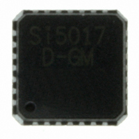
SI5017-D-GM Silicon Laboratories Inc, SI5017-D-GM Datasheet - Page 12

SI5017-D-GM
Manufacturer Part Number
SI5017-D-GM
Description
IC CLOCK/DATA RECOVERY 28MLP
Manufacturer
Silicon Laboratories Inc
Type
Clock and Data Recovery (CDR)r
Datasheet
1.SI5017-D-GM.pdf
(26 pages)
Specifications of SI5017-D-GM
Input
Differential
Output
CML
Frequency - Max
2.7GHz
Voltage - Supply
3.135 V ~ 3.465 V
Operating Temperature
-40°C ~ 85°C
Mounting Type
Surface Mount
Package / Case
28-VQFN Exposed Pad, 28-HVQFN, 28-SQFN, 28-DHVQFN
Frequency-max
2.7GHz
Lead Free Status / RoHS Status
Contains lead / RoHS non-compliant
Other names
336-1279
Si5017
4. Functional Description
The Si5017 integrates a high-speed limiting amplifier
with a CDR unit that operates between 2.4 and
2.7 Gbps. No external reference clock is required for
clock and data recovery. The limiting amplifier magnifies
very low-level input data signals so accurate clock and
data recovery can be performed. The CDR uses Silicon
Laboratories DSPLL
synchronous to the input data stream. The recovered
clock retimes the incoming data, and both are output
synchronously via current-mode logic (CML) drivers.
Silicon
superior jitter performance while eliminating the need
for external loop filter components found in traditional
phase-locked loop (PLL) implementations.
The limiting amplifier includes a control input for
adjusting the data slicing level and provides a loss-of-
signal level alarm output. The CDR includes a bit-error-
rate performance monitor which signals a high bit-error-
rate condition (associated with excessive incoming
jitter) relative to an externally adjustable bit-error-rate
threshold.
The optional reference clock minimizes the CDR
acquisition time and provides a stable reference for
maintaining the output clock when locking to reference
is desired.
4.1. Limiting Amplifier
The limiting amplifier accepts the low-level signal output
from a transimpedance amplifier (TIA). The low-level
signal is amplified to a usable level for the CDR unit.
The minimum input swing requirement is specified in
Table 2. Larger input amplitudes (up to the maximum
input swing specified in Table 2) are accommodated
without degradation of performance. The limiting
amplifier ensures optimal data slicing by using a digital
dc offset cancellation technique to remove any dc bias
introduced by the amplification stage.
4.2. DSPLL
The Si5017 PLL structure (shown in the "1. Detailed
Block Diagram" on page 4) utilizes Silicon Laboratories'
DSPLL
performance while eliminating the need for external loop
filter
implementations. This is achieved using a digital signal
processing (DSP) algorithm to replace the loop filter
commonly found in analog PLL designs. This algorithm
processes the phase detector error term and generates
a digital control value to adjust the frequency of the
voltage-controlled oscillator (VCO). This technology
enables CDR with far less jitter than is generated using
12
components
Laboratories’
technology
®
®
technology to recover a clock
found
to
DSPLL
maintain
in
technology
traditional
superior
ensures
jitter
PLL
Rev. 1.5
traditional methods, and it eliminates performance
degradation caused by external component aging. In
addition, because external loop filter components are
not required, sensitive noise entry points are eliminated,
thus making the DSPLL less susceptible to board-level
noise
compliance easier to attain in the application.
4.3. Operation Without an External Refer-
The Si5017 can perform clock and data recovery
without
REFCLK+ input to VDD and the REFCLK– input to
GND configures the device to operate without an
external reference clock. Clock recovery is achieved by
monitoring the timing quality of the incoming data
relative to the VCO frequency. Lock is maintained by
continuously monitoring the incoming data timing quality
and adjusting the VCO accordingly. Details of the lock
detection and the lock-to-reference functions while in
this mode are described in their respective sections
below.
Note: Without an external reference the acquisition of data is
4.4. Operation With an External Reference
The Si5017 can also perform clock and data recovery
with an external reference. The device’s optional
external reference clock centers the DSPLL, minimizes
the acquisition time, and maintains a stable output clock
(CLKOUT) when lock-to-reference (LTR) is asserted.
When the reference clock is present, the Si5017 uses
the reference clock to center the VCO output frequency
so that clock and data are recovered from the input data
stream. The device self configures for operation with
one of three reference clock frequencies. This
eliminates the need to externally configure the device to
operate with a particular reference clock.
The reference clock centers the VCO for a nominal
output between 2.5 and 2.7 GHz. The VCO frequency is
centered at 16, 32, or 128 times the reference clock
frequency. Detection circuitry continuously monitors the
reference clock input to determine whether the device
should be configured for a reference clock that is 1/16,
1/32, or 1/128 the nominal VCO output. Approximate
reference clock frequencies for some target applications
are given in Table 7.
ence
dependent solely on the data itself and typically
requires more time to acquire lock than when a refer-
ence is applied.
sources
an external
and
reference clock. Tying
making
SONET/SDH
jitter
the


