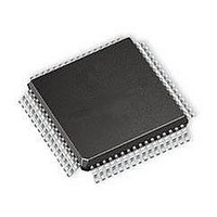
PIC16F1526-I/PT Microchip Technology, PIC16F1526-I/PT Datasheet - Page 231

PIC16F1526-I/PT
Manufacturer Part Number
PIC16F1526-I/PT
Description
MCU 14KB FLASH 768B RAM 64-TQFP
Manufacturer
Microchip Technology
Datasheet
1.PIC16F1526-IPT.pdf
(354 pages)
Specifications of PIC16F1526-I/PT
Processor Series
PIC16F
Core
PIC
Program Memory Type
Flash
Program Memory Size
14 KB
Data Ram Size
768 B
Interface Type
MI2C, SPI, EUSART
Number Of Timers
9
Operating Supply Voltage
1.8 V to 5.5 V
Maximum Operating Temperature
+ 85 C
Mounting Style
SMD/SMT
Package / Case
TQFP-64
Development Tools By Supplier
MPLAB IDE Software
Minimum Operating Temperature
- 40 C
Lead Free Status / Rohs Status
Lead free / RoHS Compliant
Available stocks
Company
Part Number
Manufacturer
Quantity
Price
Company:
Part Number:
PIC16F1526-I/PT
Manufacturer:
Microchip Technology
Quantity:
10 000
Part Number:
PIC16F1526-I/PT
Manufacturer:
MICROCHIP/微芯
Quantity:
20 000
- Current page: 231 of 354
- Download datasheet (3Mb)
21.5.8
The addressing procedure for the I
the first byte after the Start condition usually deter-
mines which device will be the slave addressed by the
master device. The exception is the general call
address which can address all devices. When this
address is used, all devices should, in theory, respond
with an Acknowledge.
The general call address is a reserved address in the
I
GCEN bit of the SSPxCON2 register is set, the slave
module will automatically ACK the reception of this
address regardless of the value stored in SSPxADD.
After the slave clocks in an address of all zeros with
the R/W bit clear, an interrupt is generated and slave
software
Figure 21-23
sequence.
FIGURE 21-24:
21.5.9
An SSPx Mask (SSPxMSK) register
available in I
held in the SSPxSR register during an address
comparison operation. A zero (‘ 0 ’) bit in the SSPxMSK
register has the effect of making the corresponding bit
of the received address a “don’t care”.
This register is reset to all ‘ 1 ’s upon any Reset
condition and, therefore, has no effect on standard
SSPx operation until written with a mask value.
The SSPx Mask register is active during:
• 7-bit Address mode: address compare of A<7:1>.
• 10-bit Address mode: address compare of A<7:0>
2011 Microchip Technology Inc.
2
C protocol, defined as address 0x00. When the
only. The SSPx mask has no effect during the
reception of the first (high) byte of the address.
GCEN (SSPxCON2<7>)
SDAx
SCLx
SSPxIF
BF (SSPxSTAT<0>)
GENERAL CALL ADDRESS SUPPORT
SSPX MASK REGISTER
can
2
C Slave mode as a mask for the value
shows
read
S
SLAVE MODE GENERAL CALL ADDRESS SEQUENCE
a
SSPxBUF
1
general
2
General Call Address
2
3
C bus is such that
(Register
and
call
4
reception
5
respond.
21-5) is
6
Preliminary
7
R/W =
8
0
ACK
In 10-bit Address mode, the UA bit will not be set on
the reception of the general call address. The slave
will prepare to receive the second byte as data, just as
it would in 7-bit mode.
If the AHEN bit of the SSPxCON3 register is set, just
as with any other address reception, the slave hard-
ware will stretch the clock after the 8th falling edge of
SCLx. The slave must then set its ACKDT value and
release the clock with communication progressing as it
would normally.
Address is compared to General Call Address
after ACK, set interrupt
9
D7
1
PIC16(L)F1526/27
D6
2
Cleared by software
SSPxBUF is read
Receiving Data
D5
3
D4
4
D3
5
D2
6
D1
7
DS41458A-page 231
D0
8
ACK
9
’1’
Related parts for PIC16F1526-I/PT
Image
Part Number
Description
Manufacturer
Datasheet
Request
R

Part Number:
Description:
IC, 8BIT MCU, PIC16F, 32MHZ, SOIC-18
Manufacturer:
Microchip Technology
Datasheet:

Part Number:
Description:
IC, 8BIT MCU, PIC16F, 32MHZ, SSOP-20
Manufacturer:
Microchip Technology
Datasheet:

Part Number:
Description:
IC, 8BIT MCU, PIC16F, 32MHZ, DIP-18
Manufacturer:
Microchip Technology
Datasheet:

Part Number:
Description:
IC, 8BIT MCU, PIC16F, 32MHZ, QFN-28
Manufacturer:
Microchip Technology
Datasheet:

Part Number:
Description:
IC, 8BIT MCU, PIC16F, 32MHZ, QFN-28
Manufacturer:
Microchip Technology
Datasheet:

Part Number:
Description:
IC, 8BIT MCU, PIC16F, 32MHZ, QFN-28
Manufacturer:
Microchip Technology
Datasheet:

Part Number:
Description:
IC, 8BIT MCU, PIC16F, 32MHZ, SSOP-20
Manufacturer:
Microchip Technology
Datasheet:

Part Number:
Description:
IC, 8BIT MCU, PIC16F, 20MHZ, DIP-40
Manufacturer:
Microchip Technology
Datasheet:

Part Number:
Description:
IC, 8BIT MCU, PIC16F, 32MHZ, QFN-28
Manufacturer:
Microchip Technology
Datasheet:

Part Number:
Description:
IC, 8BIT MCU, PIC16F, 20MHZ, MQFP-44
Manufacturer:
Microchip Technology
Datasheet:

Part Number:
Description:
IC, 8BIT MCU, PIC16F, 20MHZ, QFN-20
Manufacturer:
Microchip Technology
Datasheet:

Part Number:
Description:
IC, 8BIT MCU, PIC16F, 32MHZ, QFN-28
Manufacturer:
Microchip Technology
Datasheet:

Part Number:
Description:
7 KB Flash, 384 Bytes RAM, 32 MHz Int. Osc, 16 I/0, Enhanced Mid Range Core, Low
Manufacturer:
Microchip Technology

Part Number:
Description:
14KB Flash, 512B RAM, 256B EEPROM, LCD, 1.8-5.5V 40 UQFN 5x5x0.5mm TUBE
Manufacturer:
Microchip Technology
Datasheet:

Part Number:
Description:
14KB Flash, 512B RAM, 256B EEPROM, LCD, 1.8-5.5V 40 UQFN 5x5x0.5mm TUBE
Manufacturer:
Microchip Technology


