PIC16F1526-I/PT Microchip Technology, PIC16F1526-I/PT Datasheet - Page 195
PIC16F1526-I/PT
Manufacturer Part Number
PIC16F1526-I/PT
Description
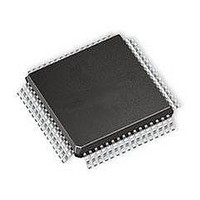
MCU 14KB FLASH 768B RAM 64-TQFP
Manufacturer
Microchip Technology
Datasheet
1.PIC16F1526-IPT.pdf
(354 pages)
Specifications of PIC16F1526-I/PT
Processor Series
PIC16F
Core
PIC
Program Memory Type
Flash
Program Memory Size
14 KB
Data Ram Size
768 B
Interface Type
MI2C, SPI, EUSART
Number Of Timers
9
Operating Supply Voltage
1.8 V to 5.5 V
Maximum Operating Temperature
+ 85 C
Mounting Style
SMD/SMT
Package / Case
TQFP-64
Development Tools By Supplier
MPLAB IDE Software
Minimum Operating Temperature
- 40 C
Lead Free Status / Rohs Status
Lead free / RoHS Compliant
Available stocks
Company
Part Number
Manufacturer
Quantity
Price
Company:

Part Number:
PIC16F1526-I/PT
Manufacturer:
Microchip Technology
Quantity:
10 000
Part Number:
PIC16F1526-I/PT
Manufacturer:
MICROCHIP/微芯
Quantity:
20 000


20.3.7
In Sleep mode, the TMRx register will not increment
and the state of the module will not change. If the CCPx
pin is driving a value, it will continue to drive that value.
When the device wakes up, TMRx will continue from its
previous state.
20.3.8
The PWM frequency is derived from the system clock
frequency. Any changes in the system clock frequency
will result in changes to the PWM frequency. See
Section 5.0 “Oscillator Module (With Fail-Safe
Clock Monitor)”
TABLE 20-9:
2011 Microchip Technology Inc.
APFCON
CCP1CON
CCP2CON
CCP3CON
CCP4CON
CCP5CON
CCP6CON
CCP7CON
CCP8CON
CCP9CON
CCP10CON
INTCON
PIE1
PIE2
PIE3
PIE4
PIR1
PIR2
PIR3
PIR4
PR2
PR4
PR6
PR8
PR10
T2CON
T4CON
T6CON
Legend: — = Unimplemented location, read as ‘ 0 ’. Shaded cells are not used by the PWM.
Name
*
Page provides register information.
OPERATION IN SLEEP MODE
CHANGES IN SYSTEM CLOCK
FREQUENCY
Timer2 Period Register
Timer4 Period Register
Timer6 Period Register
Timer8 Period Register
Timer10 Period Register
TMR1GIE
TMR1GIF
CCP10IE
CCP10IF
CCP6IE
CCP6IF
OSFIE
OSFIF
Bit 7
GIE
for additional details.
—
—
—
—
—
—
—
—
—
—
—
—
—
—
SUMMARY OF REGISTERS ASSOCIATED WITH STANDARD PWM
TMR5GIE
TMR5GIF
CCP5IE
CCP9IE
CCP5IF
CCP9IF
PEIE
ADIE
ADIF
Bit 6
—
—
—
—
—
—
—
—
—
—
—
TMR3GIE
TMR3GIF
TMR0IE
CCP4IE
CCP4IF
RC1IE
RC2IE
RC1IF
RC2IF
Bit 5
T2OUTPS<3:0>
T4OUTPS<3:0>
T6OUTPS<3:0>
—
DC10B<1:0>
DC1B<1:0>
DC2B<1:0>
DC3B<1:0>
DC4B<1:0>
DC5B<1:0>
DC6B<1:0>
DC7B<1:0>
DC8B<1:0>
DC9B<1:0>
CCP3IE
CCP3IF
Preliminary
TX1IE
TX2IE
TX1IF
TX2IF
INTE
Bit 4
—
—
—
TMR6IE
CCP8IE
TMR6IF
SSP1IE
BCL1IE
SSP1IF
CCP8IF
BCL1IF
IOCIE
20.3.9
Any Reset will force all ports to Input mode and the
CCP registers to their Reset states.
20.3.10
This module incorporates I/O pins that can be moved to
other locations with the use of the alternate pin function
register, APFCON. To determine which pins can be
moved and what their default locations are upon a
Reset, see
more information.
Bit 3
—
PIC16(L)F1526/27
TMR10IE
TMR10IF
TMR2ON
TMR4ON
TMR6ON
TMR5IE
TMR0IF
CCP1IE
CCP7IE
CCP1IF
TMR5IF
CCP7IF
Section 12.1 “Alternate Pin Function”
EFFECTS OF RESET
ALTERNATE PIN LOCATIONS
Bit 2
—
CCP10M<3:0>
CCP1M<3:0>
CCP2M<3:0>
CCP3M<3:0>
CCP4M<3:0>
CCP5M<3:0>
CCP6M<3:0>
CCP7M<3:0>
CCP8M<3:0>
CCP9M<3:0>
T3CKISEL
TMR2IE
TMR8IE
TMR4IE
TMR2IF
TMR8IF
TMR4IF
BCL2IE
BCL2IF
INTF
Bit 1
T2CKPS<:0>1
T4CKPS<:0>1
T6CKPS<:0>1
CCP2SEL
TMR1IE
CCP2IE
TMR3IE
TMR1IF
TMR3IF
SSP2IE
CCP2IF
SSP2IF
IOCIF
Bit 0
DS41458A-page 195
Register
on Page
179*
179*
179*
179*
179*
197
197
197
197
197
197
197
197
197
197
176
176
176
118
80
81
82
83
84
85
86
87
88
for
Related parts for PIC16F1526-I/PT
Image
Part Number
Description
Manufacturer
Datasheet
Request
R

Part Number:
Description:
IC, 8BIT MCU, PIC16F, 32MHZ, SOIC-18
Manufacturer:
Microchip Technology
Datasheet:

Part Number:
Description:
IC, 8BIT MCU, PIC16F, 32MHZ, SSOP-20
Manufacturer:
Microchip Technology
Datasheet:

Part Number:
Description:
IC, 8BIT MCU, PIC16F, 32MHZ, DIP-18
Manufacturer:
Microchip Technology
Datasheet:

Part Number:
Description:
IC, 8BIT MCU, PIC16F, 32MHZ, QFN-28
Manufacturer:
Microchip Technology
Datasheet:

Part Number:
Description:
IC, 8BIT MCU, PIC16F, 32MHZ, QFN-28
Manufacturer:
Microchip Technology
Datasheet:
Part Number:
Description:
IC, 8BIT MCU, PIC16F, 32MHZ, QFN-28
Manufacturer:
Microchip Technology
Datasheet:
Part Number:
Description:
IC, 8BIT MCU, PIC16F, 32MHZ, SSOP-20
Manufacturer:
Microchip Technology
Datasheet:

Part Number:
Description:
IC, 8BIT MCU, PIC16F, 20MHZ, DIP-40
Manufacturer:
Microchip Technology
Datasheet:

Part Number:
Description:
IC, 8BIT MCU, PIC16F, 32MHZ, QFN-28
Manufacturer:
Microchip Technology
Datasheet:

Part Number:
Description:
IC, 8BIT MCU, PIC16F, 20MHZ, MQFP-44
Manufacturer:
Microchip Technology
Datasheet:

Part Number:
Description:
IC, 8BIT MCU, PIC16F, 20MHZ, QFN-20
Manufacturer:
Microchip Technology
Datasheet:
Part Number:
Description:
IC, 8BIT MCU, PIC16F, 32MHZ, QFN-28
Manufacturer:
Microchip Technology
Datasheet:
Part Number:
Description:
7 KB Flash, 384 Bytes RAM, 32 MHz Int. Osc, 16 I/0, Enhanced Mid Range Core, Low
Manufacturer:
Microchip Technology

Part Number:
Description:
14KB Flash, 512B RAM, 256B EEPROM, LCD, 1.8-5.5V 40 UQFN 5x5x0.5mm TUBE
Manufacturer:
Microchip Technology
Datasheet:
Part Number:
Description:
14KB Flash, 512B RAM, 256B EEPROM, LCD, 1.8-5.5V 40 UQFN 5x5x0.5mm TUBE
Manufacturer:
Microchip Technology