CMF10120D Cree Inc, CMF10120D Datasheet - Page 9
CMF10120D
Manufacturer Part Number
CMF10120D
Description
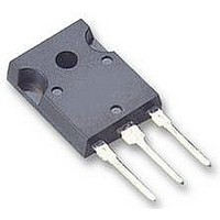
SIC MOSFET N-CH 1200V 24A TO247
Manufacturer
Cree Inc
Series
Z-FET™r
Specifications of CMF10120D
Fet Type
SiCFET N-Channel, Silicon Carbide
Fet Feature
Standard
Rds On (max) @ Id, Vgs
220 mOhm @ 10A, 20V
Drain To Source Voltage (vdss)
1200V (1.2kV)
Current - Continuous Drain (id) @ 25° C
24A
Vgs(th) (max) @ Id
4V @ 500µA
Gate Charge (qg) @ Vgs
47.1nC @ 20V
Input Capacitance (ciss) @ Vds
928pF @ 800V
Power - Max
152W
Mounting Type
*
Package / Case
*
Transistor Polarity
N Channel
Continuous Drain Current Id
24A
Drain Source Voltage Vds
1.2kV
On Resistance Rds(on)
0.16ohm
Rds(on) Test Voltage Vgs
20V
Rohs Compliant
YES
Configuration
Single
Resistance Drain-source Rds (on)
160 mOhms
Forward Transconductance Gfs (max / Min)
3.7 S, 3.4 S
Drain-source Breakdown Voltage
1200 V
Gate-source Breakdown Voltage
25 V
Continuous Drain Current
24 A
Power Dissipation
152 W
Mounting Style
Through Hole
Gate Charge Qg
47.1 nC
Lead Free Status / Rohs Status
Lead free / RoHS Compliant


9
As shown, minimizing L
dampening. Minimizing L
strongly recommended that the gate drive be located as close to the SiC DMOSFET
as possible to minimize L
characterize this device. Lower values of external gate resistance can be used so
long as the gate pulse fidelity is maintained. In the event that no external gate
resistance is used, it is suggested that the gate current be checked to indirectly
verify that there is no ringing present in the gate circuit. This can be accomplished
with a very small current transformer. A recommended setup is a two-stage
current transformer as shown below:
The two stage current transformer first stage consists of 10 turns of AWG 30 wire
on a small high permeability core. A Ferroxcube 3E27 material is recommended.
The second stage is a small wide bandwidth current transformer, such as the
Tektronix CT-2. Lastly, a separate source return should be used for the gate drive
as shown below:
V
CMF10120D Rev. -
PULSE
GATE DRIVE INPUT
R
LOOP
LOOP
LOOP
LOOP
LOOP
LOOP
LOOP
L
LOOP
minimizes the value of R
minimizes the value of R
. An external resistance of 6.8 Ω was used to
. An external resistance of 6.8 Ω was used to
also minimizes the rise/fall time. Therefore, it is
also minimizes the rise/fall time. Therefore, it is
VCC
VEE
+
-
GATE DRIVER
C
GATE
IG SENSE
T1
LOOP
LOOP
R
R
LOOP
LOOP
needed for critical
2
needed for critical
C
L
2
SiC DMOSFET
LOOP
GATE
C
L
LOOP
GATE
1
Related parts for CMF10120D
Image
Part Number
Description
Manufacturer
Datasheet
Request
R

Part Number:
Description:
CREE PLCC4 SMD LED WHITE
Manufacturer:
Cree Inc
Datasheet:
Part Number:
Description:
CREE PLCC4 SMD LED WHITE
Manufacturer:
Cree Inc
Datasheet:

Part Number:
Description:
CREE PLCC4 SMD LED WHITE
Manufacturer:
Cree Inc
Datasheet:
Part Number:
Description:
CREE PLCC4 SMD LED WHITE
Manufacturer:
Cree Inc
Datasheet:
Part Number:
Description:
CREE PLCC4 SMD LED WHITE
Manufacturer:
Cree Inc
Datasheet:

Part Number:
Description:
DIODE SCHOTTKY 600V 16.5A TO-247
Manufacturer:
Cree Inc
Datasheet:

Part Number:
Description:
DIODE SCHOTTKY 600V 6A TO220-2
Manufacturer:
Cree Inc
Datasheet:
Part Number:
Description:
DIODE SCHOTTKY 600V 10A TO220-2
Manufacturer:
Cree Inc
Datasheet:

Part Number:
Description:
IC AMP MMIC HEMT 25W 780019PKG
Manufacturer:
Cree Inc
Datasheet:

Part Number:
Description:
Cree� XLamp� XT-E LEDs
Manufacturer:
CREE [Cree, Inc]
Datasheet:
Part Number:
Description:
Cree� EZBright290� LEDs
Manufacturer:
CREE [Cree, Inc]
Datasheet:

Part Number:
Description:
DIODE SCHOT 600V 2A ZREC TO220
Manufacturer:
Cree Inc
Datasheet:
Part Number:
Description:
DIODE SCHOT 600V 3A ZREC TO252
Manufacturer:
Cree Inc
Datasheet: