NHD-2.23-12832UCB3 Newhaven Display, NHD-2.23-12832UCB3 Datasheet - Page 9
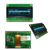
NHD-2.23-12832UCB3
Manufacturer Part Number
NHD-2.23-12832UCB3
Description
LCD OLED GRAPHIC 128 X 32 BLUE
Manufacturer
Newhaven Display
Datasheet
1.NHD-2.23-12832UCB3.pdf
(14 pages)
Specifications of NHD-2.23-12832UCB3
Pixel Density
128 x 32
Viewing Area (w X H)
60 mm x 18 mm
Operating Voltage
2.85 V
Operating Current
28 mA
Maximum Operating Temperature
+ 85 C
Minimum Operating Temperature
- 40 C
Illumination Color
Blue
Viewing Angle
80 deg
Lead Free Status / Rohs Status
Lead free / RoHS Compliant


Bank17 to Bank32
(Page 1)
Set Segment
Remap
Entire Display ON
Set Normal/
Inverse Display
Set Multiplex
Ratio
Dim mode setting
Master
configuration
Set Display ON/
OFF
Set Page Start
Address
Set COM Output
Scan Direction
Set Display Offset
Set Display Clock
Divide Ratio /
Oscillator
Frequency
Set Area Color
Mode ON/OFF &
Low Power
Display Mode
Set Pre‐charge
0
0
0
0
0
0
0
0
0
0
0
0
0
A0/A1
A4/A5
A6/A7
B0~B7
A[7:0]
B[7:0]
C[7:0]
D[7:0]
A[5:0]
A[3:0]
B[7:0]
C[7:0]
C0/C8
A[5:0]
A[7:0]
X[5:0]
AC/
AE/
AD
A8
AB
AE
AF
D3
D5
D8
D9
D7
A7
B7
C7
B7
C7
A7
1
1
1
1
*
1
*
1
1
1
1
1
1
*
1
1
0
1
A6
B6
C6
D6
B6
C6
A6
0
0
0
0
*
0
*
0
0
0
0
1
1
*
1
1
0
1
A5
B5
D5
A5
B5
A5
A5
X5
C5
C5
1
1
1
1
1
*
1
0
1
1
0
0
0
0
0
A4
D4
A4
A4
A4
B4
C4
B4
C4
X4
0
0
0
0
0
*
0
0
0
1
0
1
1
1
1
A3
D3
A3
A3
A3
A3
B3
C3
B3
C3
X3
0
0
0
1
1
1
1
1
0
0
0
1
0
1
D2
A2
B2
C2
A2
A2
B2
C2
X2
A2
A2
X2
0
1
1
0
1
1
1
0
0
1
0
0
0
A1
B1
C1
D1
A1
A1
B1
C1
A1
X1
A1
A1
[9]
0
0
1
0
1
0
1
0
1
0
0
0
0
A0
B0
D0
X0
X0
X0
A0
A0
B0
A0
X0
A0
A0
X0
C0
C0
0
1
1
0
0
1
1
0
1
A,B,C, and D.
A[1:0] : 00b, 01b, 10b, or 11b for Color = A, B, C, or D of BANK17.
A[3:2] : 00b, 01b, 10b, or 11b for Color = A, B, C, or D of BANK18.
.
.
.
D[5:4] : 00b, 01b, 10b, or 11b for Color = A, B, C, or D of BANK31.
D[7:6] : 00b, 01b, 10b, or 11b for Color = A, B, C, or D of BANK32.
X[0] = 0; Column address 0 is mapped to SEG0
X[0] = 1; Column address 131 is mapped to SEG0
X[0] = 0; Resume RAM content display. Output follows RAM content.
X[0] = 1; Entire display ON. Output ignores RAM content.
X[0] = 0; Normal display.
X[0] = 1; Inverse display.
Set MUX ratio to N+1 MUX
N=A[5:0]; from 16MUX to 64MUX (0 to 14 are invalid)
A[3:0] = reserved. Set as 0000b
B[7:0] = Set contrast for BANK0. Range 0‐255d. Refer to command
81h.
C[7:0] = Set brightness for color bank. Range 0‐255d. Refer to
command 82h.
Selects external VCC supply
ACh = Display ON in dim mode
AEh = Display OFF (sleep mode)
AFh = Display ON in normal mode
Set GDRAM Page Start Address for Page Addressing Mode using X[2:0].
PAGE0~PAGE7
X[3] = 0; Normal mode. Scan from COM0 to COM[N‐1]
X[3] = 1; Remapped mode. Scan from COM[N‐1] to COM0
Set vertical shift by COM from 0~63.
A[3:0] = Define the divide ratio of the display clocks.
Divide ratio = A[3:0] +1
A[7:4] = Set the Oscillator Frequency. Frequency increases with the
value of A[7:4]. Range 0000b~1111b.
X[5:4] = 00b; Monochrome mode
X[5:4] = 11b; Area Color mode
X[2] = 0 and X[0] = 0; Normal power mode
X[2] = 1 and X[0] = 1; Set low power display mode
A[3:0] = Phase 1 period of up to 15 DCLK clocks. 0 is invalid.
A[7:4] = Phase 2 period of up to 15 DCLK clocks. 0 is invalid.
0000b
0111b
AEh
AEh
64
00
00
2h
2h
0
0
0
0
0
Related parts for NHD-2.23-12832UCB3
Image
Part Number
Description
Manufacturer
Datasheet
Request
R

Part Number:
Description:
LCD OLED GRAPHIC 128 X 32 YLW
Manufacturer:
Newhaven Display
Datasheet:

Part Number:
Description:
DISPLAY VFD ALPHA 1X20 6.5MM
Manufacturer:
Newhaven Display
Datasheet:

Part Number:
Description:
DISPLAY VFD ALPHA 1X16 5MM
Manufacturer:
Newhaven Display
Datasheet:

Part Number:
Description:
DISPLAY VFD 7-SEG 1X9 9.7MM
Manufacturer:
Newhaven Display
Datasheet:

Part Number:
Description:
DISPLAY VFD 7-SEG 1X6 20MM
Manufacturer:
Newhaven Display
Datasheet:

Part Number:
Description:
DISPLAY VFD 7-SEG 1X19 11MM
Manufacturer:
Newhaven Display
Datasheet:

Part Number:
Description:
DISPLAY VFD 7-SEG 1X3 8MM
Manufacturer:
Newhaven Display
Datasheet:

Part Number:
Description:
DISPLAY VFD CUSTOM DVD
Manufacturer:
Newhaven Display
Datasheet:

Part Number:
Description:
DISPLAY VFD CUST AUDIO
Manufacturer:
Newhaven Display
Datasheet:

Part Number:
Description:
DISPLAY VFD CUST AUDIO
Manufacturer:
Newhaven Display
Datasheet:

Part Number:
Description:
DISPLAY VFD 7-SEG 1X5 7.6MM
Manufacturer:
Newhaven Display
Datasheet:

Part Number:
Description:
DISPLAY VFD CUST APPLIANCE
Manufacturer:
Newhaven Display
Datasheet:

Part Number:
Description:
DISPLAY VFD CUSTOM DVD
Manufacturer:
Newhaven Display
Datasheet:

Part Number:
Description:
DISPLAY VFD 7-SEG 1X4 7.6MM
Manufacturer:
Newhaven Display
Datasheet:

Part Number:
Description:
DISPLAY VFD 7-SEG 1X9 8MM
Manufacturer:
Newhaven Display
Datasheet: