NHD-2.23-12832UCB3 Newhaven Display, NHD-2.23-12832UCB3 Datasheet
NHD-2.23-12832UCB3
Specifications of NHD-2.23-12832UCB3


Related parts for NHD-2.23-12832UCB3


NHD-2.23-12832UCB3 Summary of contents
Page 1
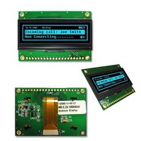
... NHD‐2.23‐12832UCB3 OLED Display Module NHD‐ Newhaven Display 2.23‐ 2.23” diagonal size 12832‐ 128 x 32 pixel resolution UC‐ ...
Page 2
Document Revision History Revision Date 0 5/1/2011 Functions and Features • 128 x 32 pixel resolution • Built‐in SSD1305 controller • Parallel or serial MPU interface • Single, low voltage power supply • RoHS compliant Description Initial Product Release [2] Changed by ‐ ...
Page 3
... Mechanical Drawing Newhaven Display NHD-2.23-12832UCB3 [3] ...
Page 4
Interface Description Parallel Interface: Pin No. Symbol External Connection 1 VSS Power Supply 2 VDD Power Supply 3 NC ‐ 4 D/C MPU 5 R/W or /WR MPU 6 E or /RD MPU 7‐14 DB0 – DB7 MPU 15 NC ‐ 16 /RES MPU 17 /CS MPU 18 NC ‐ ...
Page 5
I2C Interface: Pin No. Symbol External Connection 1 VSS Power Supply 2 VDD Power Supply 3 NC ‐ 4 SA0 MPU 5‐6 VSS Power Supply 7 SCL MPU 8 SDA MPU IN 9 SDA MPU OUT 10‐14 VSS Power Supply 15 NC ‐ 16 ...
Page 6
Wir ring Diagrams [6] ...
Page 7
Electrical Characteristics Item Operating Temperature Range Storage Temperature Range Supply Voltage Supply Current (logic) Supply Current (display) Sleep Mode Current “H” Level input “L” Level input “H” Level output “L” Level output Optical Characteristics Item Viewing Angle – Vertical (top) Viewing Angle – Vertical (bottom) Viewing Angle – Horizontal (left) Viewing Angle – Horizontal (right) Contrast Ratio Response Time (rise) Response Time (fall) Brightness Lifetime Note: Lifetime at typical temperature is based on accelerated high‐temperature operation. Lifetime is ...
Page 8
Built‐in SSD1305 controller. Instruction Table Instruction D/C HEX DB7 DB6 Set Lower Column 0 00~ 0F 0 Start Address Set Higher 0 10~1F 0 Column Start Address Set Memory 0 20 0 Addressing Mode A[1:0] * Set Column 0 21 0 Address A[7:0] A7 A6 B[7:0] B7 B6 Set Page Address 0 22 0 ...
Page 9
Bank17 to Bank32 A[7:0] A7 A6 (Page 1) B[7:0] B7 B6 C[7:0] C7 C6 D[7:0] D7 D6 Set Segment 0 A0/A1 1 Remap Entire Display ON 0 A4/A5 1 Set Normal/ 0 A6/A7 1 Inverse Display Set Multiplex 0 A8 1 Ratio A[5:0] * Dim mode setting 0 AB 1 A[3:0] ...
Page 10
Period A[7:0] A7 A6 Set COM pins 0 DA 1 Hardware X[5:4] 0 configuration Set VCOMH 0 DB 1 Deselect Level A[5:2] 0 Enter Read 0 E0 1 Modify Write mode NOP 0 E3 1 Exit Read Modify 0 EE 1 Write mode For detailed instruction information, see datasheet: http://www.newhavendisplay.com/app_notes/SSD1305.pdf ...
Page 11
MPU Interface For detailed timing information, see datasheet: http://www.newhavendisplay.com/app_notes/SSD1305.pdf 6800‐MPU Parallel Interface The parallel interface consists of 8 bi‐directional data pins, R/W, D/C, E, and /CS. A LOW on R/W indicates write operation, and HIGH on R/W indicates read operation. A LOW on D/C indicates “Command” read or write, and HIGH on D/C indicates “Data” read or write. The E input serves as data latch signal, while /CS is LOW. Data is latched at the falling edge of E signal. Function Write Command Read Status Write Data Read Data 8080‐MPU Parallel Interface The parallel interface consists of 8 bi‐directional data pins, /RD, /WR, D/C, and /CS. A LOW on D/C indicates “Command” read or write, and HIGH on D/C indicates “Data” read or write. A rising edge of /RS input serves as a data read latch signal while /CS is LOW. A rising edge of /WR input serves as a data/command write latch signal while /CS is LOW. Function Write Command Read Status Write Data Read Data Alternatively, /RD and /WR can be kept stable while /CS serves as the data/command latch signal. Function Write Command Read Status Write Data Read Data ...
Page 12
Serial Interface The serial interface consists of serial clock SCLK, serial data SDIN, D/C, and /CS. D0 acts as SCLK and D1 acts as SDIN. D2 should be left open. D3~D7, E, and R/W should be connected to GND. Function Write Command Write Data SDIN is shifted into an 8‐bit shift register on every rising edge of SCLK in the order of D7, D6,…D0. D/C is sampled on every eighth clock and the data byte in the shift register is written to the GDRAM or command register in the same clock. Note: Read is not available in serial mode. C Interface The I2C interface consists of a slave address bit SA0, I2C‐bus data signal SDA, and I2C‐bus clock signal SCL. D1 and D2 can be tied together, and act as SDA. D0 acts as SCL. Both the data and clock signals must be connected to pull‐up resistors. /RES is used to initialize the device. Note: SA0 bit allows the device to have a slave address of either “0111100” or “0111101”. Note: Data and acknowledgement are sent through the SDA. The ITO track resistance and the pull‐up resistance at SDA becomes a voltage potential divider. As a result, it may not be possible to attain a valid logic “0” level on SDA for the ACK signal. SDA signal will be ignored on the I2C bus. For detailed protocol information, see datasheet: http://www.newhavendisplay.com/app_notes/SSD1305.pdf ...
Page 13
Example Initialization Sequence: Set_Display_On_Off(0x00); Set_Display_Clock(0x10); Set_Multiplex_Ratio(0x1F); Set_Display_Offset(0x00); Set_Start_Line(0x00); Set_Master_Config(0x00); Set_Area_Color(0x05); Set_Addressing_Mode(0x02); Set_Segment_Remap(0x01); Set_Common_Remap(0x08); Set_Common_Config(0x10); Set_LUT(0x3F,0x3F,0x3F,0x3F); Set_Contrast_Control(Brightness); Set_Area_Brightness(Brightness); Set_Precharge_Period(0xD2); Set_VCOMH(0x08); ...
Page 14
Quality Information Test Item High Temperature storage Test the endurance of the display at high storage temperature. Low Temperature storage Test the endurance of the display at low storage temperature. High Temperature Test the endurance of the display by Operation applying electric stress (voltage & current) at high temperature. Low Temperature Test the endurance of the display by Operation applying electric stress (voltage & current) at low temperature. High Temperature / Test the endurance of the display by Humidity Operation applying electric stress (voltage & current) at high temperature with high humidity. Thermal Shock resistance Test the endurance of the display by applying electric stress (voltage & current) during a cycle of low and high temperatures. Vibration test Test the endurance of the display by applying vibration to simulate transportation and use. Atmospheric Pressure test Test the endurance of the display by applying atmospheric pressure to simulate transportation by air. Static electricity test Test the endurance of the display by applying electric static discharge. ...