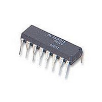
PCF8591P NXP Semiconductors, PCF8591P Datasheet - Page 7

PCF8591P
Manufacturer Part Number
PCF8591P
Description
IC, A/D AND D/A CONVERTER, 8BIT, 16-DIP
Manufacturer
NXP Semiconductors
Type
General Purposer
Specifications of PCF8591P
Number Of Channels
1
Number Of Adc's
1
Number Of Dac's
1
Adc/dac Resolution
8b
Interface Type
Serial (I2C)
Operating Supply Voltage (typ)
3.3/5V
Sample Rate
11.1KSPS
Number Of Adc Inputs
4
Number Of Dac Outputs
1
Operating Supply Voltage (max)
6V
Operating Supply Voltage (min)
2.5V
Operating Temperature (max)
85C
Operating Temperature (min)
-40C
Pin Count
16
Mounting
Through Hole
Supply Voltage Range
2.5V To 6V
Operating Temperature Range
-40°C To +85°C
Digital Ic Case Style
DIP
No. Of Pins
16
Linearity Error -
1.5LSB
Termination Type
DIP
Supply Voltage Max
8V
Input Channels Per Adc
1
Rohs Compliant
Yes
Filter Terminals
DIP
Conversion Time
90µs
Data Interface
I2C, Serial
Lead Free Status / RoHS Status
Compliant
Available stocks
Company
Part Number
Manufacturer
Quantity
Price
Company:
Part Number:
PCF8591P
Manufacturer:
SANYO
Quantity:
20 200
Company:
Part Number:
PCF8591P
Manufacturer:
NXP
Quantity:
5 510
Philips Semiconductors
7.3
The third byte sent to a PCF8591 device is stored in the
DAC data register and is converted to the corresponding
analog voltage using the on-chip D/A converter. This D/A
converter consists of a resistor divider chain connected to
the external reference voltage with 256 taps and selection
switches. The tap-decoder switches one of these taps to
the DAC output line (see Fig.6).
The analog output voltage is buffered by an auto-zeroed
unity gain amplifier. This buffer amplifier may be switched
on or off by setting the analog output enable flag of the
2003 Jan 27
handbook, full pagewidth
8-bit A/D and D/A converter
D/A conversion
AGND
V REF
Fig.6 DAC resistor divider chain.
R256
R255
R3
R2
R1
7
control register. In the active state the output voltage is
held until a further data byte is sent.
The on-chip D/A converter is also used for successive
approximation A/D conversion. In order to release the
DAC for an A/D conversion cycle the unity gain amplifier is
equipped with a track and hold circuit. This circuit holds the
output voltage while executing the A/D conversion.
The output voltage supplied to the analog output AOUT is
given by the formula shown in Fig.7. The waveforms of a
D/A conversion sequence are shown in Fig.8.
FF
02
01
00
DAC out
DECODER
TAP
MBL826
D7
D6
D0
Product specification
PCF8591


