LCBS-8-01 Richco Plastic Co, LCBS-8-01 Datasheet
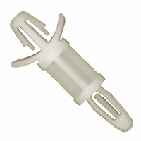
LOCKING BOARD SUPPORT 1/2"

LCBS-8-01

Manufacturer Part Number
LCBS-8-01
Description
LOCKING BOARD SUPPORT 1/2"
Manufacturer
Richco Plastic Co
Series
LCBSr
Datasheets

Specifications of LCBS-8-01

Holding Type
Arrowhead, Snap Lock
Length
1.229" (31.22mm)
Between Board Height
0.500" (12.70mm) 1/2"
Mounting Type
Arrowhead, Snap-Lock, Winged
Support Hole Diameter
0.156" (3.96mm) 5/32"
Support Panel Thickness
0.062" (1.57mm) 1/16"
Mounting Hole Diameter
0.187" (4.75mm) 3/16"
Mounting Panel Thickness
0.031 ~ 0.078" (0.79 ~ 1.98mm)
Overall Length
12.7mm
Spacer Material
Nylon
External Width
7.1mm
Spacing Height
12.7mm
Body Diameter
4.75mm
Spacer Style
PC Board
Color
Natural
Diameter
0.28 in.
Diameter, Mounting Hole
0.156 in. ±0.003 in. Dia. Hole in a 0.82 in. Thick Board, 0.187 in. ±0.003 in. Dia. Hole in a 1⁄16 in. (Nominal) Thick Panel⁄Chassis
Size, Thread
7⁄32
Lead Free Status / RoHS Status
Lead free / RoHS Compliant
Lead Free Status / RoHS Status
Lead free / RoHS Compliant, Lead free / RoHS Compliant
Other names
LCBS-8
RP430
FEATURES
ORDERING INFORMATION
DS1202
DS1202S
DS1202S–8
DS1202N
DS1202SN
DS1202SN–8 8–pin SOIC (IND)
DESCRIPTION
The DS1202 Serial Timekeeping Chip contains a real
time clock/calendar and 24 bytes of static RAM. It com-
municates with a microprocessor via a simple serial in-
terface. The real time clock/calendar provides seconds,
minutes, hours, day, date, month, and year information.
The end of the month date is automatically adjusted for
months with less than 31 days, including corrections for
leap year. The clock operates in either the 24–hour or
12–hour format with an AM/PM indicator. Interfacing the
All Rights Reserved. For important information regarding
patents and other intellectual property rights, please refer to
Dallas Semiconductor data books.
Real time clock counts seconds, minutes, hours, date
of the month, month, day of the week, and year with
leap year compensation valid up to 2100
24 x 8 RAM for scratchpad data storage
Serial I/O for minimum pin count
2.0–5.5 volt full operation
Uses less than 300 nA at 2 volts
Single–byte or multiple–byte (burst mode) data trans-
fer for read or write of clock or RAM data
8–pin DIP or optional 16–pin SOIC for surface mount
Simple 3–wire interface
TTL–compatible (V
Optional industrial temperature range –40 C to +85 C
(IND)
Copyright 1997 by Dallas Semiconductor Corporation.
8–pin DIP
16–pin SOIC
8–pin SOIC
8–pin DIP (IND)
16–pin SOIC (IND)
CC
= 5V)
PIN ASSIGNMENT
PIN DESCRIPTION
NC
X1, X2
GND
RST
I/O
SCLK
V
DS1202 with a microprocessor is simplified by using
synchronous serial communication. Only three wires
are required to communicate with the clock/RAM: (1)
RST (Reset), (2) I/O (Data line), and (3) SCLK (Serial
clock). Data can be transferred to and from the clock/
RAM one byte at a time or in a burst of up to 24 bytes.
The DS1202 is designed to operate on very low power
and retain data and clock information on less than 1 mi-
crowatt.
CC
Serial Timekeeping Chip
GND
NC
NC
NC
NC
NC
X1
X2
GND
GND
NC
– No Connection
– 32.768 KHz Crystal Input
– Ground
– Reset
– Data Input/Output
– Serial Clock
– Power Supply Pin
X1
X2
NC
X1
X2
DS1202, DS1202S
1
2
3
4
5
6
7
8
16–PIN SOIC
8–PIN SOIC
8–PIN DIP
1
2
3
4
(208 mil)
1
2
3
4
8
7
6
5
8
7
6
5
16
15
14
13
12
10
11
9
V
SCLK
I/O
RST
CC
V
SCLK
I/O
RST
CC
DS1202, DS1202S
V
NC
SCLK
NC
I/O
NC
NC
RST
CC
032697 1/11

Related parts for LCBS-8-01

LCBS-8-01 Summary of contents

Page 1

FEATURES Real time clock counts seconds, minutes, hours, date of the month, month, day of the week, and year with leap year compensation valid up to 2100 RAM for scratchpad data storage Serial I/O for minimum pin ...

Page 2

DS1202, DS1202S OPERATION The main elements of the Serial Timekeeper are shown in Figure 1: shift register, control logic, oscillator, real time clock, and RAM. To initiate any transfer of data, RST is taken high and eight bits are loaded ...

Page 3

RESET AND CLOCK CONTROL All data transfers are initiated by driving the RST input high. The RST input serves two functions. First, RST turns on the control logic which allows access to the shift register for the address/command sequence. Second, ...

Page 4

DS1202, DS1202S REGISTER SUMMARY A register data format summary is shown in Figure 4. CRYSTAL SELECTION A 32.768 KHz crystal, can be directly connected to the DS1202 via pins 2 and 3 (X1, X2). The crystal selected for use should ...

Page 5

REGISTER ADDRESS/DEFINITION Figure 4 REGISTER ADDRESS A. CLOCK SEC MIN ...

Page 6

DS1202, DS1202S ABSOLUTE MAXIMUM RATINGS* Voltage on Any Pin Relative to Ground Operating Temperature Storage Temperature Soldering Temperature * This is a stress rating only and functional operation of the device at these or any other conditions above those indicated ...

Page 7

AC ELECTRICAL CHARACTERISTICS PARAMETER SYMBOL Data to CLK Setup Data to CLK Setup CLK to Data Hold CLK to Data Hold t t CDH CDH CLK to Data Delay t CLK to Data Delay t CDD ...

Page 8

DS1202, DS1202S TIMING DIAGRAM: READ DATA TRANSFER Figure 5 RESET t CC CLOCK t CDH t DC DATA INPUT/ 0 OUTPUT TIMING DIAGRAM: WRITE DATA TRANSFER Figure 6 RESET CLOCK t CDH t DC DATA INPUT/ ...

Page 9

I is specified with RST, I/O, and SCLK open. The clock halt flag must be set to logic one (oscillator disabled). CC2 11. At power–up, RST must logic 0 until logic one state. ...

Page 10

DS1202, DS1202S DS1202S SERIAL TIMEKEEPER 16–PIN SOIC 032697 10/11 F phi H J PKG 16–PIN DIM MIN MAX A IN. 0.500 0.511 MM 12.70 12.99 B IN. 0.290 0.300 MM 7.37 7.65 C ...

Page 11

DS1202S8 8–PIN SOIC 200 MIL DS1202, DS1202S J F 0–8 deg. typ. L PKG 8–PIN DIM MIN MAX A IN. 0.203 0.213 MM 5.16 5.41 B IN. 0.203 0.213 MM 5.16 5.41 ...

Related keywords