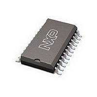
CBTS3384D-T NXP Semiconductors, CBTS3384D-T Datasheet - Page 4

CBTS3384D-T
Manufacturer Part Number
CBTS3384D-T
Description
Manufacturer
NXP Semiconductors
Datasheet
1.CBTS3384D-T.pdf
(11 pages)
Specifications of CBTS3384D-T
Logic Family
CBT
Number Of Bits
10
Number Of Elements
2
Technology
CMOS
High Level Output Current
-128mA
Low Level Output Current
128mA
On Resistance
10Ohm
Operating Temp Range
-40C to 85C
Operating Temperature Classification
Industrial
Operating Supply Voltage (min)
4.5V
Operating Supply Voltage (typ)
5V
Operating Supply Voltage (max)
5.5V
Quiescent Current
3uA
Pin Count
24
Mounting
Surface Mount
Lead Free Status / RoHS Status
Compliant
Philips Semiconductors
DC ELECTRICAL CHARACTERISTICS
NOTES:
1. All typical values are at V
2. This is the increase in supply current for each input that is at the specified TTL voltage level rather than V
3. Measured by the voltage drop between the A and the B terminals at the indicated current through the switch. On-state resistance is
AC CHARACTERISTICS
GND = 0 V; t
NOTE:
1. This parameter is warranted but not production tested. The propagation delay is based on the RC time constant of the typical on-state
NOTE:
1. This parameter is warranted but not production tested. The propagation delay is based on the RC time constant of the typical on-state
2002 Dec 13
SYMBOL
C
10-bit bus switch with 5-bit output enables
and Schottky undershoot protection
determined by the lowest voltage of the two (A or B) terminals.
resistance of the switch and a load capacitance of 50 pF, when driven by an ideal voltage source (zero output impedance).
resistance of the switch and a load capacitance of 50 pF, when driven by an ideal voltage source (zero output impedance); at +25 °C.
∆I
I
I(OFF)
r
SYMBOL
I
UCP
V
V
on
on
CC
C
SYMBOL
I
CC
IK
I
P
I
3
t
t
t
dis
pd
en
t
t
t
t
t
PZH
PHZ
PZL
PLZ
PD
Input clamp voltage
Input leakage current
Quiescent supply current
Additional supply current per input pin
Control pins
Power-off leakage current
On-resistance
Pass voltage
Undershoot static current protection
R;
C
L
= 50 pF
Propagation delay
Output enable time
to High and Low level
Output disable time
from High and Low level
Propagation delay (see Note 1)
Output enable time to High level
Output enable time from High level
Output enable time to Low level
Output enable time from Low level
PARAMETER
CC
= 5 V, T
PARAMETER
PARAMETER DESCRIPTION
1
2
amb
= 25 °C.
2
V
V
V
V
or GND
V
V
V
V
V
V
V
CC
CC
CC
CC
I
O
CC
CC
CC
I
CC
= 3.0 V or 0
= V
= 3.0 V or 0, OE = V
= 4.5 V; I
= 5.5 V; V
= 5.5 V; I
= 5.5 V, one input at 3.4 V, other inputs at V
= 4.5 V; V
= 4.5 V; V
= 4.5 V; V
= 5.0 V, I
CC
= 5.0 V; I
(INPUT)
FROM
A or B
OE
OE
B
I
O
I
I
I
I
= -18 mA
TEST CONDITIONS
= 400 µA; OE = 5.0 V; V
= GND or 5.5 V
= 0 V; I
= 0 V; I
= 2.4 V; I
= 0, V
4
O
= -100 µA
I
= V
I
I
CC
= 64 mA
= 30 mA
I
= -15 mA
CC
(OUTPUT)
B or A
A or B
A or B
or GND
TO
MIN.
1.6
1.7
2.3
2.5
—
B
≥ 3.0 V
V
CC
-40 to +85° C
V
Min
1.0
1.0
—
CC
CC
= 5 V, ±0.5 V
LIMITS
MEAN
= +5.0 V ±0.5 V
3.4
3.3
4.5
—
4
LIMITS
CC
Min
T
3.4
or GND.
—
—
—
—
—
—
—
—
—
—
amb
= -40 to +85 °C
Max
0.25
LIMITS
5.7
5.2
Typ
3.6
—
—
—
—
10
10
4
5
5
8
CBTS3384
MAX.
1
250
5.6
5.5
6.6
6
Max
-1.2
2.5
3.9
±1
15
—
—
—
3
7
7
Product data
UNIT
ns
ns
ns
UNIT
UNIT
pS
nS
nS
nS
nS
mA
mA
µA
µA
pF
pF
V
Ω
V


