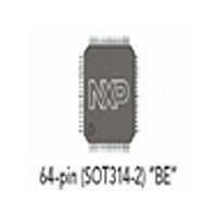
SAA7111AHZ NXP Semiconductors, SAA7111AHZ Datasheet - Page 10

SAA7111AHZ
Manufacturer Part Number
SAA7111AHZ
Description
Manufacturer
NXP Semiconductors
Datasheet
1.SAA7111AHZ.pdf
(72 pages)
Specifications of SAA7111AHZ
Pin Count
64
Package Type
LQFP
Lead Free Status / RoHS Status
Compliant
Available stocks
Company
Part Number
Manufacturer
Quantity
Price
Company:
Part Number:
SAA7111AHZ
Manufacturer:
TI
Quantity:
6 710
Company:
Part Number:
SAA7111AHZ
Manufacturer:
NXP
Quantity:
34
Company:
Part Number:
SAA7111AHZ
Manufacturer:
SHARP
Quantity:
1
Company:
Part Number:
SAA7111AHZ
Manufacturer:
NXP
Quantity:
5 690
Part Number:
SAA7111AHZ
Manufacturer:
PHILIPS/飞利浦
Quantity:
20 000
Company:
Part Number:
SAA7111AHZ/V4,557
Manufacturer:
NXP Semiconductors
Quantity:
10 000
Philips Semiconductors
8
8.1
The SAA7111A offers four analog signal inputs, two
analog main channels with source switch, clamp circuit,
analog amplifier, anti-alias filter and video CMOS ADC
(see Fig.5).
8.2
The anti-alias filters are adapted to the line-locked clock
frequency via a filter control circuit. During the vertical
blanking time, gain and clamping control are frozen.
8.2.1
The clamp control circuit controls the correct clamping of
the analog input signals. The coupling capacitor is also
used to store and filter the clamping voltage. An internal
digital clamp comparator generates the information with
respect to clamp-up or clamp-down. The clamping levels
for the two ADC channels are fixed for luminance (60) and
chrominance (128). Clamping time in normal use is set
with the HCL pulse at the back porch of the video signal.
8.2.2
Signal (white) peak control limits the gain at signal
overshoots. The flow charts (see Figs 13 and 14) show
more details of the AGC. The influence of supply voltage
variation within the specified range is automatically
eliminated by clamp and automatic gain control.
The gain control circuit receives (via the I
gain levels for the two analog amplifiers or controls one of
these amplifiers automatically via a built-in automatic gain
control (AGC) as part of the Analog Input Control (AICO).
1998 May 15
handbook, halfpage
Enhanced Video Input Processor (EVIP)
Fig.3
FUNCTIONAL DESCRIPTION
Analog input processing
Analog control circuits
255
C
G
60
1
LAMPING
AIN CONTROL
Analog line with clamp (HCL) and gain
range (HSY).
analog line blanking
GAIN
HSY
TV line
CLAMP
HCL
2
MGL065
C-bus) the static
10
The AGC (automatic gain control for luminance) is used to
amplify a CVBS or Y signal to the required signal
amplitude, matched to the ADCs input voltage range.
The AGC active time is the sync bottom of the video signal.
8.3
The 8-bit chrominance signal is fed to the multiplication
inputs of a quadrature demodulator, where two subcarrier
signals from the local oscillator DTO1 are applied
(0 and 90 phase relationship to the demodulator axis).
The frequency is dependent on the present colour
standard. The output signals of the multipliers are
low-pass filtered (four programmable characteristics) to
achieve the desired bandwidth for the colour difference
signals (PAL and NTSC) or the 0 and 90 FM-signals
(SECAM).
The colour difference signals are fed to the
Brightness/Contrast/Saturation block (BCS), which
includes the following five functions:
handbook, halfpage
AGC (Automatic Gain Control for chrominance
PAL and NTSC)
Chrominance amplitude matching (different gain factors
for R
Cr and Cb for all standards)
Chrominance saturation control
Luminance contrast and brightness
Limiting YUV to the values 1 (min.) and 254 (max.) to
fulfil CCIR-601 requirements.
(1 V(p-p) 27/47 )
Chrominance processing
Y and B
4.5 dB
7.5 dB
Fig.4 Automatic gain range.
analog input level
0 dB
Y to achieve CCIR-601 levels
maximum
minimum
range tbf
Product specification
ADC input level
MGG063
SAA7111A
controlled
0 dB


