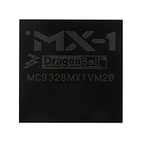
MC9328MX1VM20 Freescale, MC9328MX1VM20 Datasheet - Page 59

MC9328MX1VM20
Manufacturer Part Number
MC9328MX1VM20
Description
Manufacturer
Freescale
Datasheet
1.MC9328MX1VM20.pdf
(100 pages)
Specifications of MC9328MX1VM20
Operating Temperature (min)
0C
Operating Temperature (max)
70C
Operating Temperature Classification
Commercial
Mounting
Surface Mount
Lead Free Status / RoHS Status
Compliant
Available stocks
Company
Part Number
Manufacturer
Quantity
Price
Company:
Part Number:
MC9328MX1VM20
Manufacturer:
Freescale Semiconductor
Quantity:
10 000
Company:
Part Number:
MC9328MX1VM20R2
Manufacturer:
Freescale Semiconductor
Quantity:
10 000
4.4.4
4.5
The specifications for the pen ADC are shown in
Freescale Semiconductor
LD[15:0]
1
2
3
4
5
Symbol
Pen ADC Specifications
HSYN
Maximum frequency of LCDC_CLK is 48 MHz, which is controlled by Peripheral Clock Divider Register.
Maximum frequency of SCLK is HCLK / 5, otherwise LD output will be wrong.
VSYN, HSYN and SCLK can be programmed as active high or active low. In the above timing diagram, all
these 3 signals are active high.
Tpix is the pixel clock period which equals LCDC_CLK period * (PCD + 1).
Ts is the shift clock period. Ts = Tpix * (panel data bus width).
VSYN
SCLK
Non-TFT Panel Timing
T1
T2
T3
T4
HSYN to VSYN delay
HSYN pulse width
VSYN to SCLK
SCLK to HSYN
Parameter
T2
1
Full Range Resolution
Non-Linearity Error
Accuracy
Table 17. Non TFT Panel Timing Diagram
Table 18. Pen ADC System Performance
Tested under input = 0~1.8V at 25°C
Figure 33. Non-TFT Panel Timing
3
MC9328MX1 Technical Data, Rev. 7
T1
1
T3
1
Minimum Value
Allowed Register
Table 18
1
0
0
–
0
XMAX
through
1, 2
Functional Description and Application Information
13 bits
4 bits
9 bits
Table
Ts
20.
Actual Value
0 ≤ T3 ≤ Ts
HWIDTH+1
HWAIT2+2
HWAIT1+1
T4
5
T2
Tpix
Unit
Tpix
Tpix
–
T1
4
59


