L6204 STMicroelectronics, L6204 Datasheet
L6204
Specifications of L6204
Available stocks


Related parts for L6204


L6204 Summary of contents
Page 1
... TTL/CMOS COMPATIBLE DRIVER HIGH EFFICIENCY CHOPPING MULTIPOWER BCD TECHNOLOGY DESCRIPTION The L6204 is a dual full bridge driver for motor control applications realized in BCD technology which combines isolated DMOS power transistors with CMOS and Bipolar circuits on the same chip. By using mixed technology it has been possible to optimize the logic circuitry and the power stage to achieve the best possible performance ...
Page 2
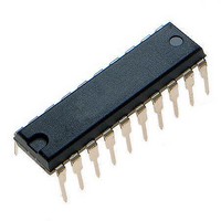
... L6204 PIN CONNECTIONS SENS1 1 20 IN1 2 19 ENABLE1 3 18 OUT1 4 17 GND 5 16 GND 6 15 OUT3 7 14 ENABLE2 8 13 IN3 9 12 SENSE2 10 11 DIP20 DIP16+2+2 PIN DESCRIPTION SO DIP Pin Symbols Pin (*) 1 1 SENSE IN1 3 3 ENABLE OUT GND 8 6 GND 9 7 OUT 3 ...
Page 3
... EN1 = EN2 = L OFF ON IN1 = IN2 = IN3 = IN4 = EN1 = EN2 = L IN1 = IN2 = IN3 = IN4 = EN1 = EN2 = H Value 50 -0 1.23 2 -40 to 150 SO DIP Max 16 14 Max 73 65 Min. Typ. Max 150 500 1 1.2 -0.3 0 -10 50 L6204 Unit Unit C/W C/W Unit KHz 3/12 ...
Page 4
... OSCILLATOR D2 C2 CIRCUIT DESCRIPTION L6204 is a dual full bridge IC designed to drive DC motors, stepper motors and other inductive loads. Each bridge has 4 power DMOS transistor with R (see fig. 3) The 4 half bridges can be controlled independently by means of the 4 inputs IN!, IN2, IN3, IN4 and 2 en- able inputs ENABLE1 and ENABLE2 ...
Page 5
... C1. On the low-to-high transition a spike of the same polarity is generated by C2, preceded by a spike of the opposite polarity due to the charging of the input capacity of the lower POWER DMOS transistor (see fig. 2). Figure 1. Intrinsic Structures in the POWER MOS Transistors Figure 2. Current Typical Spikes on the Sensing Pin L6204 5/12 ...
Page 6
... It is also possible to operate two or more L6204s using only 2 diodes and 2 capacitance for all the ICs; all the Vboot pins are connected to the Cs- tore capacitance while the pin 11 (VCP) of just one L6204 is connect to C have to be connected to the same V Figure 3 ...
Page 7
... A thermal protection circuit has been included that will disable the device if the junction temperature reach- es 150 °C. When the temperature has fallen to a safe level the device restarts under the control of the input and enable signals. IN1 = H IN2 = H EN1 = H IN1 = X IN2 = X EN1 = L L6204 7/12 ...
Page 8
... RC filter can be added if necessary. POWER DISSIPATION (each bridge) In order to achieve the high performance provided by the L6204 some attention must be paid to ensure that it has an adequate PCB area to dissipate the heat. The first stage of any thermal design is to calculate the dissipated power in the appl ication, for this example the half step operation shown in figure 7 is con- sidered ...
Page 9
... TOTAL ENERGY PER CYCLE TOT OFF/ON ON The Total Power Dissipation PDIS is simply : T = Rise time time Fall Time Dead time Period · I · T ON/OFF DS(ON QUIESCENT QUIESCENT + E ) bridge COM ON/OFF OFF/ QUIESCENT DIS TOT · 2/3 f · V · )bridge COM ON/OFF d L6204 9/12 ...
Page 10
... L6204 mm DIM. MIN. TYP. MAX. a1 0.51 B 0.85 1.40 b 0.50 b1 0.38 0.50 D 24.80 E 8.80 e 2.54 e3 22.86 F 7.10 I 5.10 L 3.30 Z 1.27 10/12 inch MIN. TYP. MAX. 0.020 0.033 0.055 0.020 0.015 0.020 0.976 0.346 0.100 0.900 0.280 0.201 0.130 0.050 OUTLINE AND MECHANICAL DATA ...
Page 11
... C 0 (typ.) D 17.7 18.1 0.697 E 10 10.65 0.394 e 1.27 e3 16.51 F 7.4 7.6 0.291 L 0.4 1.27 0.016 S 8 (max.) inch MECHANICAL DATA TYP. MAX. 0.104 0.012 0.019 0.013 0.020 0.713 0.419 0.050 0.65 0.299 0.050 L6204 OUTLINE AND SO28 11/12 ...
Page 12
... L6204 Information furnished is believed to be accurate and reliable. However, STMicroelectronics assumes no responsibility for the consequences of use of such information nor for any infringement of patents or other rights of third parties which may result from its use. No license is granted by implication or otherwise under any patent or patent rights of STMicroelectronics. Specifications mentioned in this publication are subject to change without notice ...