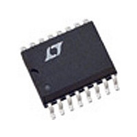
LT1054CSW#TRMPBF Linear Technology, LT1054CSW#TRMPBF Datasheet - Page 3

LT1054CSW#TRMPBF
Manufacturer Part Number
LT1054CSW#TRMPBF
Description
Manufacturer
Linear Technology
Type
Inverting/Step Upr
Datasheet
1.LT1054CSWTRMPBF.pdf
(16 pages)
Specifications of LT1054CSW#TRMPBF
Operating Supply Voltage (min)
3.5V
Operating Supply Voltage (max)
15V
Operating Temp Range
0C to 100C
Operating Temperature Classification
Commercial
Package Type
SOIC W
Pin Count
16
Mounting
Surface Mount
Output Voltage
AdjV
Output Current
100mA
Lead Free Status / RoHS Status
Compliant
Available stocks
Company
Part Number
Manufacturer
Quantity
Price
ELECTRICAL C
temperature range, otherwise specifications are at T
PARAMETER
Supply Current
Supply Voltage Range
Voltage Loss (V
Output Resistance
Oscillator Frequency
Reference Voltage
Regulated Voltage
Line Regulation
Load Regulation
Maximum Switch Current
Supply Current in Shutdown
Note 1: Absolute Maximum Ratings are those values beyond which the life
of a device may be impaired.
Note 2: The absolute maximum supply voltage rating of 16V is for
unregulated circuits using LT1054. For regulation mode circuits using
LT1054 with V
be increased to 20V. The absolute maximum supply voltage for LT1054L
is 7V.
Note 3: The devices are guaranteed by design to be functional up to the
absolute maximum junction temperature.
Note 4: For voltage loss tests, the device is connected as a voltage
inverter, with pins 1, 6, and 7 (3, 12, and 13 S package) unconnected.
The voltage losses may be higher in other configurations.
OUT
IN
– V
15V at Pin 5 (Pin 11 on S package), this rating may
OUT
)
HARA TERISTICS
C
CONDITIONS
I
LT1054
LT1054L
C
LT1054: 3.5V V
LT1054L: 3.5V V
I
V
LT1054: 7V V
V
V
LOAD
REF
IN
I
IN
IN
PIN1
I
I
I
OUT
OUT
OUT
OUT
= C
= 7V, T
= 7V, 100
= 60 A, T
= 0V
= 0mA
= 10mA to 100mA (Note 5)
= 10mA
= 100mA
= 125mA (LT1054L)
OUT
A
J
= 100 F Tantalum (Note 4)
= 25 C. (Note 7)
= 25 C, R
J
= 25 C
IN
LT1054:
LT1054L: V
The
R
IN
IN
L
12V, R
L
500 (Note 6)
15V
7V
= 500 (Note 6)
denotes specifications which apply over the full operating
L
V
V
V
= 500 (Note 6)
IN
IN
IN
IN
Note 5: Output resistance is defined as the slope of the curve, ( V
portion of the curve. The incremental slope of the curve will be higher at
currents < 10mA due to the characteristics of the switch transistors.
Note 6: All regulation specifications are for a device connected as a
positive-to-negative converter/regulator with R1 = 20k, R2 = 102.5k,
C1 = 0.002 F, (C1 = 0.05 F S package) C
C
Note 7: The S8 package uses a different die than the H, J8, N8 and S
packages. The S8 device will meet all the existing data sheet parameters.
See Regulation and Capacitor Selection in the Applications Information
section for differences in application requirements.
= 3.5V
= 15V
= 3.5V
= 7V
I
OUT
OUT
= 100 F tantalum.
), for output currents of 10mA to 100mA. This represents the linear
– 4.70
2.35
2.25
MIN
3.5
3.5
15
15
LT1054/LT1054L
– 5.00
0.35
1.10
1.35
2.50
TYP
300
100
2.5
3.0
2.5
3.0
IN
10
25
25
10
5
= 10 F tantalum,
– 5.20
MAX
0.55
1.60
1.75
2.65
2.75
200
4.0
5.0
4.0
5.0
15
15
40
35
25
50
7
OUT
UNITS
1054lfe
3
vs
kHz
kHz
mA
mA
mA
mA
mV
mV
mA
V
V
V
V
V
V
V
V
A


