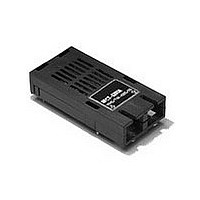
HFCT5201B Avago Technologies US Inc., HFCT5201B Datasheet - Page 2

HFCT5201B
Manufacturer Part Number
HFCT5201B
Description
Manufacturer
Avago Technologies US Inc.
Datasheet
1.HFCT5201B.pdf
(8 pages)
Specifications of HFCT5201B
Optical Fiber Type
TX/RX
Data Transfer Rate
155Mbps
Operating Temperature Classification
Commercial
Peak Wavelength
1360nm
Operating Supply Voltage (min)
4.75V
Operating Supply Voltage (typ)
5V
Operating Supply Voltage (max)
5.25V
Output Current
30mA
Operating Temp Range
0C to 70C
Pin Count
18
Lead Free Status / RoHS Status
Not Compliant
Figure 1. Block Diagram
Receiver Signal Detect
As the input optical power is decreased, Signal Detect
will switch from high to low (de‑assert point) somewhere
between sensitivity and the no light input level. As the
input optical power is increased from very low levels,
Signal Detect will switch back from low to high (assert
point). The assert level will be at least 0.5 dB higher than
the de‑assert level.
Transceiver Specified for Wide Temperature Range Op-
eration
The HFCT‑5201 is specified for operation over normal
commercial temperature range of 0° to +70°C (HF‑
CT‑5201B/D) or the extended temperature range
of ‑40° to +85°C (HFCT‑5201A/C) in an airflow of
2 m/s.
Other Members of Avago SC Duplex
155 Mb/s Product Family
• HFCT‑5205, 5103, 5215,
• XMT5370155, 1300 nm laser‑based transmitter in
• XMT5170155, 1300 nm laser‑based transmitter in
Applications Information
Typical BER Performance of Receiver versus Input Opti-
cal Power Level
The HFCT‑5201 transceiver can be operated at Bit‑Er‑
ror‑Rate conditions other than the required BER = 1 x 10
2
DATA
DATA
S IGNAL DETECT
DATA
DATA
1300 nm single mode transceivers for links up to
40 km. The part is based on the 1 x 9 industry stan‑
dard package and has an integral duplex SC con‑
nector receptacle
pigtailed package for 2 km and 15 km links with SMF
cables
pigtailed package for 40 km links with SMF cables
ELECTRICAL S UBAS S EMBLY
MONITOR
P OWER
AMP LIFIER IC
DRIVER
LAS ER
P OS T
IC
LAS ER BIAS
MONITOR
AS S EMBLIES
AMP LIFIER
P RE-
OP TICAL
TOP VIEW
LAS ER
IC
S UB-
P IN P HOTODIODE
‑
10
The typical trade‑off of BER versus Relative Input Optical
Power is shown in Figure 3. The Relative Input Optical
Power in dB is referenced to the Input Optical Power
parameter value in the Receiver Optical Characteristics
table. For BER conditions better than 1 x 10
input signal is needed (+dB).
Recommended Circuit Schematic
In order to ensure proper functionality of the HFCT‑5201
a recommended circuit is provided in Figure 4. When
designing the circuit interface, there are a few fundamen‑
tal guidelines to follow. For example, in the Recommended
Circuit Schematic figure the differential data lines should
be treated as 50 ohm Microstrip or stripline transmission
lines. This will help to minimize the parasitic inductance
and capacitance effects. Proper termination of the dif‑
ferential data signals will prevent reflections and ringing
which would compromise the signal fidelity and generate
unwanted electrical noise. Locate termination at the
received signal end of the transmission line. The length
of these lines should be kept short and of equal length.
For the high speed signal lines, differential signals should
be used, not single‑ended signals, and these differential
signals need to be loaded symmetrically to prevent un‑
balanced currents from flowing which will cause distor‑
tion in the signal.
Maintain a solid, low inductance ground plane for
returning signal currents to the power supply. Multilayer
of the ATM Forum 155.52 Mb/s Physical Layer Standard.
DUP LEX S C
RECEP TACLE
P
M
P
(R
Figure 2a. Laser Bias Monitor
Figure 2b. Power Monitor Circuit
La s e r
AC
OWER
IN
ONITOR
EF TO
9
La s e r
DC Bia s
V
E E
)
30 R
10 R
3 kΩ
V
CC
3 kΩ
3 kΩ
L
M ON
V
V
CC
EE
L
M ON
30 kΩ
(+) P in
P in 5
( - )
6
‑10
, more
1.2 V
V
R EF


