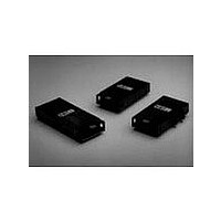
HFBR-5113 Avago Technologies US Inc., HFBR-5113 Datasheet - Page 2

HFBR-5113
Manufacturer Part Number
HFBR-5113
Description
Manufacturer
Avago Technologies US Inc.
Datasheet
1.HFBR-5113.pdf
(16 pages)
Specifications of HFBR-5113
Operating Temperature Classification
Commercial
Operating Supply Voltage (min)
4.75V
Operating Supply Voltage (typ)
5V
Operating Supply Voltage (max)
5.25V
Mounting
Through Hole
Lead Free Status / RoHS Status
Compliant
FDDI PMD standard. Likewise,
the Fast Ethernet Alliance defines
the Physical Layer for the 100
Base-FX Version of IEEE 802.3u
to be the FDDI PMD standard.
Agilent also provides several
other FDDI products compliant
with the FDDI Low Cost Fiber
(LCF) -PMD and Single Mode
(SM) -PMD standards. These
products are available with ST,
SC, and FC connector styles.
They are available in the 1x9
transceiver and 14- and 16-pin
transmitter/receiver package
styles for those designs that
require these alternate
configurations. Contact your
Agilent sales representative for
information on these alternative
FDDI products.
Transmitter Section
The transmitter section of the
HFBR-511X Series utilizes a 1300
nm surface emitting InGaAsP
LED. The LED is packaged in the
optical subassembly portion of
the transmitter section. It is dc-
coupled to a custom IC which
converts differential-input, PECL
logic signals, ECL referenced
(shifted) to a +5 V power supply,
into an analog LED drive current.
Receiver Section
The receiver section of the
HFBR-511X Series utilizes an
InGaAs PIN photodiode coupled
to a custom silicon transimped-
ance preamplifier IC. They are
packaged in the optical sub-
assembly portion of the receiver.
The PIN/preamplifier combina-
tion is ac-coupled to a custom
quantizer IC which provides the
final pulse shaping for the logic
output and the Signal Detect
function. Both the Data and
Signal Detect outputs are
DIFFERENTIAL
DATA OUT
DIFFERENTIAL
SIGNAL
DETECT OUT
DIFFERENTIAL
DATA IN
differential. Also, both Data and
Signal Detect outputs are PECL
compatible, ECL referenced
(shifted) to a +5 V power supply.
Package
The overall package concept for
the Agilent transceiver consists of
the following basic elements: two
optical subassemblies, an
electrical subassembly, and the
housing with full compliance to
the FDDI PMD standard. A block
diagram is illustrated in Figure 1.
The package outline drawings
and pin-outs are shown in Figures
2 and 3. These are compliant with
the industry standard 2x11 and
1x13 pin configurations.
The optical subassemblies utilize
a high-volume assembly process
together with low-cost lens
elements which result in a cost-
effective building block.
The electrical subassemblies
consist of a high-volume, multi-
layer printed circuit board on
which the IC chips and various
surface-mounted passive circuit
elements are attached.
Figure 1. HFBR-5111/-5112/-5113 Block Diagram.
ELECTRICAL SUBASSEMBLY
QUANTIZER IC
DRIVER IC
PREAMP
IC
2
Each transceiver package
includes internal shields for the
electrical and optical subassem-
blies to ensure low EMI emissions
and high immunity to external
EMI fields.
The outer housings including the
MIC receptacles are molded of
filled non-conductive plastic to
provide mechanical strength and
electrical isolation. The solder
posts of each package design are
isolated from the circuit design of
the transceiver and do not require
connection to a ground plane on
the circuit board.
Each transceiver is attached to its
printed circuit boards with the
2x11 or 1x13 signal pins and the
solder posts which exit the
bottom of the housing. The solder
posts provide the primary
mechanical strength to withstand
the loads imposed on the
transceiver when mating with
MIC-connectored fiber cables.
Application Information
The Applications Engineering
group of the Optical Communica-
tion Division is available to assist
you with the technical under-
PIN PHOTODIODE
OPTICAL
SUBASSEMBLIES
LED
TOP VIEW


