HFBR-5113 Avago Technologies US Inc., HFBR-5113 Datasheet
HFBR-5113
Specifications of HFBR-5113


Related parts for HFBR-5113


HFBR-5113 Summary of contents
Page 1
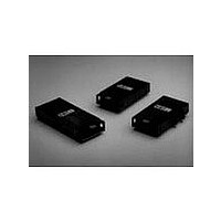
... American National Standard, ANSI X3.166 - 1990. The HFBR- 5111 represents the 2x11 package style. The “2x11” denotes two rows of eleven pins. The HFBR-5112 and HFBR-5113 represent the Narrow and Standard 1x13 package styles, respectively. The “1x13” denotes one row of thirteen pins. ...
Page 2
... Contact your Agilent sales representative for information on these alternative FDDI products. Transmitter Section The transmitter section of the HFBR-511X Series utilizes a 1300 nm surface emitting InGaAsP LED. The LED is packaged in the optical subassembly portion of the transmitter section dc- coupled to a custom IC which converts differential-input, PECL ...
Page 3
... OPTICAL REFERENCE PLANE 41.30 (1.626) 16.00 MAX. (0.630) 33.02 PLUG – REF. (1.300) MAX. Figure 2(b). HFBR-5112 Outline Drawing. 34.34 ø 1.50 1.352 4X SOLDER POSTS 0.060 30.48 0.48 1.200 22X ø LEADS 0.019 3.80 2X ø ...
Page 4
... ALL DIMENSIONS ARE NOMINAL UNLESS OTHERWISE SPECIFIED. 3. THE LEADS ARE TIN-LEAD PLATED PHOSPHOR BRONZE. 4. THE POSTS ARE TIN-LEAD PLATED BRASS. 5. THE HOUSING IS GLASS FIBER FILLED BLACK POLYETHERIMIDE. 6. THE MODULE IS SHOWN WITHOUT THE FIELD KEY INSTALLED. Figure 2(c). HFBR-5113 Outline Drawing. TOP VIEW GND 1 22 GND NC 2 ...
Page 5
FIBER OPTIC CABLE LENGTH – km Figure 4. Optical Power Budget at BOL vs. Fiber Optic Cable Length. standing ...
Page 6
... It is advised that normal static precautions be taken in the handling and assembly of these transceivers to prevent damage which may be induced by electrostatic discharge (ESD). The HFBR-511X Series meets MIL-STD-883C Method 3015.4 Class 2. Care should be taken to avoid shorting the receiver Data or Signal Detect outputs directly to ground without proper current- limiting impedance ...
Page 7
... CAUTION: DO NOT DIRECTLY CONNECT FIBER-OPTIC MODULE PECL OUTPUTS (DATA, DATA, SIGNAL DETECT, SIGNAL DETECT) TO GROUND WITHOUT PROPER CURRENT LIMITING IMPEDANCE. 7. DEVICE GROUND PINS SHOULD BE DIRECTLY AND INDIVIDUALLY CONNECTED TO GROUND. 8. DEVICE SOLDER POSTS SHOULD BE DIRECTLY CONNECTED TO PCB FOR OPTIMUM MECHANICAL SUPPORT. (b) HFBR-5112/-5113 Figure 7. Recommended Decoupling Circuit Diagram ...
Page 8
... M 3.81 NOTES: 1. TOLERANCE ± 0.05 mm, UNLESS OTHERWISE SPECIFIED. 2. SOLDER POSTS SHOULD BE CONNECTED TO PCB FOR OPTIMUM MECHANICAL SUPPORT. (c) HFBR-5113 Figure 8. Board Layout–Hole Pattern. 1.93 ± 0.15 4X 0.076 ± 0.006 0.000 M A –A– 1.04 ± 0.15 22X 0.041 ± ...
Page 9
... Electrostatic Discharge (ESD) to the MIC Receptacle Electromagnetic Interference (EMC) Immunity EN55022 (CISPR 22) in Europe and VCCI in Japan. Hence, the HFBR-511X Series of fiber optic transceivers meet the regulatory requirements listed in Table 1. Immunity Equipment utilizing these transceivers will be subject to radio-frequency electromagnetic fields in some environments. ...
Page 10
... Table 2. Ordering Information Part Number Transceivers HFBR-5111 HFBR-5112 HFBR-5113 Accessories HFBR-5001 HFBR-5198 200 3.0 180 1.5 160 2.0 3.5 140 2.5 t – TRANSMITTER r/f OUTPUT OPTICAL 3.0 RISE/FALL TIMES – ns 120 3.5 100 1200 1300 1320 1340 1360 1380 – TRANSMITTER OUTPUT OPTICAL C CENTER WAVELENGTH – ...
Page 11
... TIME – ns THE HFBR-511X OUTPUT OPTICAL PULSE SHAPE FITS WITHIN THE BOUNDARIES OF THE PULSE ENVELOPE FOR RISE AND FALL TIME MEASUREMENTS. Figure 10. Output Optical Pulse Envelope. -31.0 dBm 1 < P < -31.0 dBm) ...
Page 12
Absolute Maximum Ratings Parameter Storage Temperature Lead Soldering Temperature Lead Soldering Time Supply Voltage Data Input Voltage Differential Input Voltage Output Current Recommended Operating Conditions Parameter Ambient Operating Temperature Supply Voltage Data Input Voltage – Low Data Input Voltage – ...
Page 13
Transmitter Optical Characteristics ( 4. 5. Parameter Output Optical Power 62.5/125 0.275 Fiber Output Optical Power 50/1255 0.20 Fiber Optical Extinction ...
Page 14
... Over the specified operation voltage and temperature ranges. • With HALT Line State, (12.5 MHz square-wave), input signal. • At the end of one meter of noted optical fiber with cladding modes removed. The average power value can be converted to a peak power value by adding 3 dB. Higher output optical power transmitters are available on special request ...
Page 15
Input symbol pattern is the FDDI test pattern defined in FDDI PMD Annex A.5 with 4B/5B NRZI encoded data that contains a duty cycle base-line wander effect of 50 kHz. This sequence causes a near worst case condition for ...
Page 16
Data subject to change. Copyright © 2001 Agilent Technologies, Inc. April 4, 2001 Obsoletes 5964-9019E (11/99) 5980-1064E ...