SCD5584A OSRAM Opto Semiconductors Inc, SCD5584A Datasheet - Page 10
SCD5584A
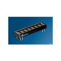
Manufacturer Part Number
SCD5584A
Description
LED Displays 5x5 Hi-Eff Green 0.145 , 8-CHARACTER
Manufacturer
OSRAM Opto Semiconductors Inc
Series
Intelligent Display®r
Datasheet
1.SCD5584A.pdf
(17 pages)
Specifications of SCD5584A
Display Type
Dot Matrix
Emitting Color
Hi-Eff. Green
Number Of Digits
8
Digit Size (in)
.145in
Viewing Area Height (mm)
3.68mm
Viewing Area Length (mm)
2.54mm
Package Type
Panel
Operating Supply Voltage (min)
4.5V
Operating Supply Voltage (typ)
5V
Operating Supply Voltage (max)
5.5V
Operating Temperature Classification
Industrial
Operating Temp Range
-40C to 85C
Mounting
Through Hole
Pin Count
10
Total Thickness (mm)
5.08mm
Opto Display Type
Panel
Pattern Type
Dot Matrix
Millicandela Rating
505µcd
Size / Dimension
1.50" L x 0.39" W x 0.20" H (38.10mm x 10.00mm x 5.08mm)
Color
Green
Configuration
5 x 5
Character Size
0.145 in
Illumination Color
High Efficiency Green
Wavelength
568 nm
Maximum Operating Temperature
+ 85 C
Minimum Operating Temperature
- 40 C
Luminous Intensity
505 ucd
Viewing Area (w X H)
2.54 mm x 3.68 mm
Lead Free Status / RoHS Status
Compliant
Voltage - Forward (vf) Typ
-
Internal Connection
-
Lead Free Status / Rohs Status
Details
Other names
Q2132089
Q68000A1000
Q68100A1000
Q68000A1000
Q68100A1000


Row Strobing
Multiplexer and Display Driver
The eight characters are row multiplexed with RAM resident col-
umn data. The strobe rate is established by the internal or external
MUX Clock rate. The MUX Clock frequency is divided by a 320
counter chain. This results in a typical strobe rate of 750 Hz. By
pulling the Clock SEL line low, the display can be operated from an
external MUX Clock. The external clock is attached to the CLK I/O
connection (pin 15). The maximum external MUX Clock frequency
should be limited to 1.0 MHz.
An asynchronous hardware Reset (pin 13) is also provided. Bring-
ing this pin low will clear the Character Address Register, Control
Word Register, RAM, and blanks the display. This action leaves the
display set at Character Address 0, and the Brightness Level set at
100%.
Thermal Considerations
The SCD558XA has been designed to provide lowest thermal
resistance from the CMOS to the ground pin.
The heat is then conducted through the traces on the users circuit
board to free air. The max. IC operating temperature is 125°C.
Maximum. IC junction temperature is calculated using the following
equation:
T
where Rθ
Rθ
soldered to the pcb or socketed and on air circulation.
Electrical & Mechanical Considerations
Interconnect Considerations
Optimum product performance can be had when the following
electrical and mechanical recommendations are adopted. The
SCD558XA’s IC is constructed in a high speed CMOS process,
consequently high speed noise on the SERIAL DATA, SERIAL
DATA CLOCK, LOAD and RESET lines may cause incorrect data
to be written into the serial shift register. Adhere to transmission
line termination procedures when using fast line drivers and long
cables (>10 cm).
Good digital grounds (pins 14, 28) and power supply decoupling
(pins 6, 9, 20, 23) will insure that I
currents do not generate localized ground bounce. Therefore it is
recommended that each display package use a 0.1 µF and 20 µF
capacitor between V
2006-01-23
J
(IC) Max.=T
PIN-A
P
will depend on ground trace thickness, whether parts are
D
J-PIN
Row
Load
Max.
=35°C/W.
A
Row 0
Row 1
Row 2
Row 3
Row 4
+(P
D
CC
Max.) (Rθ
=V
=5.5 Vx0.240=1.32 W.
and ground.
0 1 2 3 4
Load Row 0
CC
Columns
Max.x I
J-PIN
SCD5580A, SCD5581A, SCD5582A, SCD5583A, SCD5584A
CC
+Rθ
CC
(<400 mA peak) switching
Row 0
Row 1
Row 2
Row 3
Row 4
Max
PIN-A
)
0
Load Row 1
Columns
1
2 3
4
Row 0
Row 1
Row 2
Row 3
Row 4
10
0
Load Row 2
Columns
When the internal MUX Clock is being used connect the CLKSEL
pin to V
nected to the system’s reset control, it is recommended that this
pin be connected to the center node of a series 0.1 µF and 100 kΩ
RC network. Thus upon initial power up the RESET will be held
low for 10 ms allowing adequate time for the system power supply
to stabilize.
ESD Protection
The input protection structure of the SCD558XA provides signifi-
cant protection against ESD damage. It is capable of withstanding
discharges greater than 2.0 kV. Take all the standard precautions,
normal for CMOS components. These include properly grounding
personnel, tools, tables, and transport carriers that come in contact
with unshielded parts. If these conditions are not, or cannot be
met, keep the leads of the device shorted together or the parts in
anti-static packaging.
Soldering Considerations
The SCD558XA can be hand soldered with SN63 solder using a
grounded iron set to 260°C.
Wave soldering is also possible following these conditions: Pre-
heat that does not exceed 93°C on the solder side of the PC board
or a package surface temperature of 85°C. Water soluble organic
acid flux (except carboxylic acid) or rosin-based RMA flux without
alcohol can be used.
Wave temperature of 245°C ± 5°C with a dwell between 1.5 sec. to
3.0 sec. Exposure to the wave should not exceed temperatures
above 260°C for five seconds at 1.59 mm (0.063") below the seat-
ing plane. The packages should not be immersed in the wave.
Post Solder Cleaning Procedures
The least offensive cleaning solution is hot D.I. water (60 °C) for
less than 15 minutes. Addition of mild saponifiers is acceptable. Do
not use commercial dishwasher detergents.
For faster cleaning, solvents may be used. Exercise care in choos-
ing solvents as some may chemically attack the nylon package.
Maximum exposure should not exceed two minutes at elevated tem-
peratures. Acceptable solvents are TF (trichlorotrifluorethane), TA,
111 Trichloroethane, and unheated acetone.
Note:
1)
1
2
Acceptable commercial solvents are: Basic TF, Arklone, P.
Genesolv, D. Genesolv DA, Blaco-Tron TF and Blaco-Tron TA.
3
CC
4
. In those applications where RESET will not be con-
Row 0
Row 1
Row 2
Row 3
Row 4
0
Load Row 3
Columns
1
2
3 4
Row 0
Row 1
Row 2
Row 3
Row 4
0 1 2
Load Row 4
(1)
Columns
IDXX5186
3
4
Related parts for SCD5584A
Image
Part Number
Description
Manufacturer
Datasheet
Request
R

Part Number:
Description:
Manufacturer:
OSRAM Opto Semiconductors Inc
Datasheet:

Part Number:
Description:
INTELLIGENT DISP 4CHAR 5X7 HERED
Manufacturer:
OSRAM Opto Semiconductors Inc
Datasheet:

Part Number:
Description:
DISPLAY 8DIGIT CERAMIC GREEN
Manufacturer:
OSRAM Opto Semiconductors Inc
Datasheet:

Part Number:
Description:
EMITTER IR 950NM 5MM SMD RADIAL
Manufacturer:
OSRAM Opto Semiconductors Inc
Datasheet:

Part Number:
Description:
LED TOPLED GREEN 570NM 2-PLCC
Manufacturer:
OSRAM Opto Semiconductors Inc
Datasheet:

Part Number:
Description:
INTERRUPTER RELFECT W/FILTR SMD
Manufacturer:
OSRAM Opto Semiconductors Inc
Datasheet:

Part Number:
Description:
LED Displays 5x7 Green 0.145 , 4-CHARACTER
Manufacturer:
OSRAM Opto Semiconductors Inc
Datasheet:
Part Number:
Description:
Q65110A4321_SIDELED PURE GREEN EOL150407
Manufacturer:
OSRAM Opto Semiconductors Inc
Datasheet:
Part Number:
Description:
Q65110A1202_RO DETECTOR 3/5MM_TR_RO
Manufacturer:
OSRAM Opto Semiconductors Inc
Datasheet:
Part Number:
Description:
INTELLIGENT DISP 4CHAR 5X7 HERED
Manufacturer:
OSRAM Opto Semiconductors Inc
Datasheet:
Part Number:
Description:
LED TOPLED GREEN 570NM 2-PLCC
Manufacturer:
OSRAM Opto Semiconductors Inc
Datasheet:

Part Number:
Description:
PHOTODIODE 900NM 3MM W/FILTER
Manufacturer:
OSRAM Opto Semiconductors Inc
Datasheet:

Part Number:
Description:
PHOTODIODE 850NM THRU-HOLE
Manufacturer:
OSRAM Opto Semiconductors Inc
Datasheet:

Part Number:
Description:
PHOTODIODE 880NM W/FILTER SMD
Manufacturer:
OSRAM Opto Semiconductors Inc
Datasheet: