PDSP1884 OSRAM Opto Semiconductors Inc, PDSP1884 Datasheet - Page 10
PDSP1884
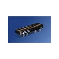
Manufacturer Part Number
PDSP1884
Description
LED Displays 5x7 Hi-Eff Green 0.18 , 8-CHARACTER
Manufacturer
OSRAM Opto Semiconductors Inc
Series
Alphanumeric Programmable Display™r
Datasheet
1.PDSP1880.pdf
(15 pages)
Specifications of PDSP1884
Display Type
Dot Matrix
Emitting Color
Hi-Eff. Green
Number Of Digits
8
Digit Size (in)
.18in
Viewing Area Height (mm)
4.57mm
Viewing Area Length (mm)
2.54mm
Package Type
Panel
Operating Supply Voltage (min)
4.5V
Operating Supply Voltage (typ)
5V
Operating Supply Voltage (max)
5.5V
Operating Temperature Classification
Industrial
Operating Temp Range
-40C to 85C
Mounting
Through Hole
Pin Count
24
Total Thickness (mm)
5.33mm
Opto Display Type
Panel
Pattern Type
Dot Matrix
Millicandela Rating
500µcd
Size / Dimension
1.69" L x 0.45" W x 0.21" H (42.93mm x 11.43mm x 5.33mm)
Color
Green
Configuration
5 x 7
Character Size
0.18 in
Illumination Color
High Efficiency Green
Wavelength
568 nm
Maximum Operating Temperature
+ 85 C
Minimum Operating Temperature
- 40 C
Luminous Intensity
500 ucd
Viewing Area (w X H)
2.54 mm x 4.57 mm
Lead Free Status / RoHS Status
Compliant
Voltage - Forward (vf) Typ
-
Internal Connection
-
Lead Free Status / Rohs Status
Details
Other names
Q68000A9109
Available stocks
Company
Part Number
Manufacturer
Quantity
Price
Company:

Part Number:
PDSP1884
Manufacturer:
NEC
Quantity:
2 000


The display Blink works the same way as the Flash Enable but
causes all twenty column drivers to cycle at 2.0 Hz thereby making
all eight digits blink at 2.0 Hz.
The Self Test function of the IC consists of two internal routines
which exercise major portions of the IC and illuminates all the
LEDs.
Clear bit clears the character RAM and writes a blank into the dis-
play memory. It however does not clear the control word.
ASCII Data or Control Word Data can be written into the display
at this point. For multiple display operation, CLK I/O must be
properly selected. CLK I/O will output the internal clock if CLK-
SEL=1, or will allow input from an external clock if CLKSEL=0.
Character RAM
The Character RAM is selected when FL , A4 and A3 are set to
1,1,1 during a read or write cycle. The Character RAM is a 8 by 8
bit RAM with each of the eight locations corresponding to a digit on
the display. Digit 0 is on the left side of the display and digit 7 is on
the right side of the display. Address lines, A2–A0 select the digit
address with A2 being the most significant bit and A0 being the
least significant bit. The two types of data stored in the Character
RAM are the ASCII coded data and the UDC Address Data. The
type of data stored in the Character RAM is determined by data bit,
D7. If D7 is low, then ASCII coded data is stored in data bits D6–
D0. If D7 is high, then UDC Address Data is stored in data bit D3–
D0.
The ASCII coded data is a 7 bit code used to select one of 128
ASCII characters permanently stored in the ASCII ROM.
The UDC Address data is a 4 bit code used to select one of the
UDC characters in the UDC RAM. There are up to 16 characters
available. See Table „Character RAM Access Logic“ (page 10).
Character RAM Access Logic
RST
1
1
1
1
UDC Address Register and UDC Character RAM
RST
1
1
1
1
2006-03-30
CE
0
0
0
0
CE
0
0
0
0
WR
0
1
0
1
WR
0
1
0
1
RD
1
0
1
0
RD
1
0
1
0
PDSP1880, PDSP1881, PDSP1882, PDSP1883, PDSP1884
FL
1
1
1
1
FL
1
1
1
1
A4
1
1
0
0
A4
0
0
0
0
A3
1
1
0
0
A3
0
0
1
1
A2
Character Address for
Digits 0–7
Character Address for
Digits 0–7
Character Address for
Digits 0–7
Character Address for
Digits 0–7
A2
Not used for UDC
Address Register
Not used for UDC
Address Register
A2–A0=Character
Row Address
A2–A0=Character
Row Address
10
UDC Address Register and UDC RAM
The UDC Address Register and UDC RAM allows the user to gen-
erate and store up to 16 custom characters. Each custom charac-
ter is defined in 5 x 7 dot matrix pattern. It takes 8 write cycles to
define a custom character, one cycle to load the UDC Address
Register and 7 cycles to define the character. The contents of the
UDC Address Register will store the 4 bit address for one of the 16
UDC RAM locations. The UDC RAM is used to store the custom
character.
UDC Address Register
The UDC Address Register is selected by setting FL=1, A4=0,
A3=0. It is a 4 bit register and uses data bits, D3–D0 to store the
4 bit address code (D7–D4 are ignored). The address code
selects one of 16 UDC RAM locations for custom character gen-
eration.
UDC RAM
The UDC RAM is selected by setting FL=1, A4=0, A3=1. The RAM
is comprised of a 7 x 5 bit RAM. As shown in Table „UDC Charac-
ter Map“ (page 11), address lines, A2-A0 select one of the 7 rows
of the custom character. Data bits, D4-D0 determine the 5 bits of
column data in each row. Each data bit corresponds to a LED. If
the data bit is high, then the LED is on. If the data bit is low, the
LED is off. To create a character, each of the 7 rows of column
data need to be defined. See Table „UDC Address Register and
UDC RAM“ (page 10) for logic.
A1
A1
A0
A0
D7 D6 D5 D4 D3 D2 D1 D0
0
0
1
1
D7 D6 D5 D4 D3 D2 D1 D0
D3–D0=UDC RAM Address Code
for Write Cycle
D3–D0=UDC RAM Address Code
for Read Cycle
D4–D0=Character Column Data
for Write Cycle
D4–D0=Character Column Data
read during a Read Cycle
7 bit ASCII code for a Write Cycle
7 bit ASCII code read during a Read Cycle
D3–D0=UDC address for a Write Cycle
D3–D0=UDC address for Read Data
UDC
Address
Register
UDC
RAM
Related parts for PDSP1884
Image
Part Number
Description
Manufacturer
Datasheet
Request
R

Part Number:
Description:
INTELLIGENT DISP 4CHAR 5X7 HERED
Manufacturer:
OSRAM Opto Semiconductors Inc
Datasheet:

Part Number:
Description:
DISPLAY 8DIGIT CERAMIC GREEN
Manufacturer:
OSRAM Opto Semiconductors Inc
Datasheet:

Part Number:
Description:
EMITTER IR 950NM 5MM SMD RADIAL
Manufacturer:
OSRAM Opto Semiconductors Inc
Datasheet:

Part Number:
Description:
LED TOPLED GREEN 570NM 2-PLCC
Manufacturer:
OSRAM Opto Semiconductors Inc
Datasheet:

Part Number:
Description:
INTERRUPTER RELFECT W/FILTR SMD
Manufacturer:
OSRAM Opto Semiconductors Inc
Datasheet:

Part Number:
Description:
LED Displays 5x7 Green 0.145 , 4-CHARACTER
Manufacturer:
OSRAM Opto Semiconductors Inc
Datasheet:

Part Number:
Description:
Q65110A4321_SIDELED PURE GREEN EOL150407
Manufacturer:
OSRAM Opto Semiconductors Inc
Datasheet:
Part Number:
Description:
Q65110A1202_RO DETECTOR 3/5MM_TR_RO
Manufacturer:
OSRAM Opto Semiconductors Inc
Datasheet:

Part Number:
Description:
PHOTODIODE 900NM 3MM W/FILTER
Manufacturer:
OSRAM Opto Semiconductors Inc
Datasheet:
Part Number:
Description:
INTELLIGENT DISP 4CHAR 5X7 HERED
Manufacturer:
OSRAM Opto Semiconductors Inc
Datasheet:
Part Number:
Description:
LED TOPLED GREEN 570NM 2-PLCC
Manufacturer:
OSRAM Opto Semiconductors Inc
Datasheet:
Part Number:
Description:
PHOTODIODE 900NM 3MM W/FILTER
Manufacturer:
OSRAM Opto Semiconductors Inc
Datasheet:

Part Number:
Description:
PHOTODIODE 850NM THRU-HOLE
Manufacturer:
OSRAM Opto Semiconductors Inc
Datasheet:

Part Number:
Description:
PHOTODIODE 880NM W/FILTER SMD
Manufacturer:
OSRAM Opto Semiconductors Inc
Datasheet: