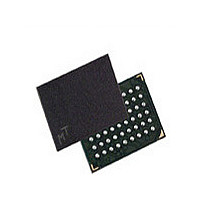
MT48LC4M16A2B4-75:G Micron Technology Inc, MT48LC4M16A2B4-75:G Datasheet - Page 32

MT48LC4M16A2B4-75:G
Manufacturer Part Number
MT48LC4M16A2B4-75:G
Description
Manufacturer
Micron Technology Inc
Type
SDRAMr
Datasheet
1.MT48LC4M16A2B4-75G.pdf
(72 pages)
Specifications of MT48LC4M16A2B4-75:G
Organization
4Mx16
Density
64Mb
Address Bus
14b
Access Time (max)
6/5.4ns
Maximum Clock Rate
133MHz
Operating Supply Voltage (typ)
3.3V
Package Type
VFBGA
Operating Temp Range
0C to 70C
Operating Supply Voltage (max)
3.6V
Operating Supply Voltage (min)
3V
Supply Current
140mA
Pin Count
54
Mounting
Surface Mount
Operating Temperature Classification
Commercial
Lead Free Status / RoHS Status
Compliant
Available stocks
Company
Part Number
Manufacturer
Quantity
Price
Company:
Part Number:
MT48LC4M16A2B4-75:G
Manufacturer:
MICRON
Quantity:
5 000
Company:
Part Number:
MT48LC4M16A2B4-75:G
Manufacturer:
MICRON21
Quantity:
859
Part Number:
MT48LC4M16A2B4-75:G
Manufacturer:
MICRON/镁光
Quantity:
20 000
Figure 21:
Figure 22:
PDF: 09005aef80725c0b/Source: 09005aef806fc13c
64MSDRAM_2.fm - Rev. N 12/08 EN
Random WRITE Cycles
WRITE-to-READ
Note:
Note:
COMMAND
COMMAND
ADDRESS
ADDRESS
Each WRITE command may be to any bank. DQM is LOW.
The WRITE command may be to any bank, and the READ command may be to any bank.
DQM is LOW. CL = 2 for illustration.
CLK
CLK
DQ
DQ
TRANSITIONING DATA
WRITE
BANK,
BANK,
COL n
WRITE
COL n
D
T0
D
T0
n
n
IN
IN
WRITE
BANK,
n + 1
COL a
NOP
D
T1
T1
D
a
IN
IN
TRANSITIONING DATA
WRITE
BANK,
COL x
BANK,
COL b
READ
T2
T2
D
x
IN
32
DON’T CARE
WRITE
COL m
BANK,
T3
T3
NOP
D
m
IN
Micron Technology, Inc., reserves the right to change products or specifications without notice.
NOP
D
T4
OUT
b
DON’T CARE
NOP
T5
b + 1
D
OUT
64Mb: x4, x8, x16 SDRAM
©2000 Micron Technology, Inc. All rights reserved.
Commands


