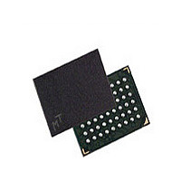
MT48LC16M16A2BG-7E IT:D Micron Technology Inc, MT48LC16M16A2BG-7E IT:D Datasheet - Page 33

MT48LC16M16A2BG-7E IT:D
Manufacturer Part Number
MT48LC16M16A2BG-7E IT:D
Description
Manufacturer
Micron Technology Inc
Type
SDRAMr
Datasheet
1.MT48LC16M16A2BG-7E_ITD.pdf
(92 pages)
Specifications of MT48LC16M16A2BG-7E IT:D
Organization
16Mx16
Density
256Mb
Address Bus
15b
Access Time (max)
5.4ns
Maximum Clock Rate
143MHz
Operating Supply Voltage (typ)
3.3V
Package Type
VFBGA
Operating Temp Range
-40C to 85C
Operating Supply Voltage (max)
3.6V
Operating Supply Voltage (min)
3V
Supply Current
135mA
Pin Count
54
Mounting
Surface Mount
Operating Temperature Classification
Industrial
Lead Free Status / RoHS Status
Compliant
- Current page: 33 of 92
- Download datasheet (3Mb)
NO OPERATION (NOP)
LOAD MODE REGISTER (LMR)
ACTIVE
Figure 13: ACTIVE Command
PDF: 09005aef8091e6d1
256Mb_sdr.pdf - Rev. N 1/10 EN
The NO OPERATION (NOP) command is used to perform a NOP to the selected device
(CS# is LOW). This prevents unwanted commands from being registered during idle or
wait states. Operations already in progress are not affected.
The mode registers are loaded via inputs A[n:0] (where An is the most significant ad-
dress term), BA0, and BA1(see Mode Register (page 46)). The LOAD MODE REGISTER
command can only be issued when all banks are idle and a subsequent executable com-
mand cannot be issued until
The ACTIVE command is used to activate a row in a particular bank for a subsequent
access. The value on the BA0, BA1 inputs selects the bank, and the address provided
selects the row. This row remains active for accesses until a PRECHARGE command is
issued to that bank. A PRECHARGE command must be issued before opening a differ-
ent row in the same bank.
BA0, BA1
Address
RAS#
CAS#
WE#
CKE
CLK
CS#
HIGH
Bank address
Row address
t
33
MRD is met.
Don’t Care
Micron Technology, Inc. reserves the right to change products or specifications without notice.
256Mb: x4, x8, x16 SDRAM
© 1999 Micron Technology, Inc. All rights reserved.
Commands
Related parts for MT48LC16M16A2BG-7E IT:D
Image
Part Number
Description
Manufacturer
Datasheet
Request
R

Part Number:
Description:
IC SDRAM 64MBIT 133MHZ 54TSOP
Manufacturer:
Micron Technology Inc
Datasheet:

Part Number:
Description:
IC SDRAM 64MBIT 5.5NS 86TSOP
Manufacturer:
Micron Technology Inc
Datasheet:

Part Number:
Description:
IC SDRAM 64MBIT 200MHZ 86TSOP
Manufacturer:
Micron Technology Inc
Datasheet:

Part Number:
Description:
IC SDRAM 64MBIT 133MHZ 54TSOP
Manufacturer:
Micron Technology Inc
Datasheet:

Part Number:
Description:
IC SDRAM 128MBIT 133MHZ 54TSOP
Manufacturer:
Micron Technology Inc
Datasheet:

Part Number:
Description:
IC SDRAM 256MBIT 133MHZ 90VFBGA
Manufacturer:
Micron Technology Inc
Datasheet:

Part Number:
Description:
IC SDRAM 128MBIT 133MHZ 54TSOP
Manufacturer:
Micron Technology Inc
Datasheet:

Part Number:
Description:
IC SDRAM 256MBIT 133MHZ 54TSOP
Manufacturer:
Micron Technology Inc
Datasheet:

Part Number:
Description:
IC DDR SDRAM 512MBIT 6NS 66TSOP
Manufacturer:
Micron Technology Inc
Datasheet:

Part Number:
Description:
IC SDRAM 128MBIT 167MHZ 86TSOP
Manufacturer:
Micron Technology Inc
Datasheet:

Part Number:
Description:
IC SDRAM 128MBIT 143MHZ 86TSOP
Manufacturer:
Micron Technology Inc
Datasheet:

Part Number:
Description:
SDRAM 256M-BIT 1.8V 54-PIN VFBGA
Manufacturer:
Micron Technology Inc
Datasheet:

Part Number:
Description:
IC SDRAM 128MBIT 143MHZ 86TSOP
Manufacturer:
Micron Technology Inc
Datasheet:

Part Number:
Description:
IC SDRAM 128MBIT 125MHZ 54VFBGA
Manufacturer:
Micron Technology Inc
Datasheet:

Part Number:
Description:
IC SDRAM 128MBIT 125MHZ 54VFBGA
Manufacturer:
Micron Technology Inc
Datasheet:


