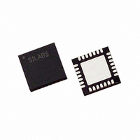
CP2102-GMR Silicon Laboratories Inc, CP2102-GMR Datasheet - Page 10

CP2102-GMR
Manufacturer Part Number
CP2102-GMR
Description
USB to UART Bridge 28-Pin QFN T/R
Manufacturer
Silicon Laboratories Inc
Specifications of CP2102-GMR
Package
28QFN
Operating Temperature
-40 to 85 °C
Applications
USB
Interface
UART
Voltage - Supply
3 V ~ 3.6 V
Package / Case
28-VQFN Exposed Pad, 28-HVQFN, 28-SQFN, 28-DHVQFN
Mounting Type
Surface Mount
Maximum Operating Temperature
+ 125 C
Minimum Operating Temperature
- 55 C
Mounting Style
SMD/SMT
Operating Supply Voltage
3.6 V
Supply Current (max)
100 mA
Lead Free Status / RoHS Status
Lead free / RoHS Compliant
For Use With
336-1161 - KIT EVALUATION FOR CP2102
Lead Free Status / Rohs Status
Details
Other names
336-1802-2
CP2102-GMR
Q4435029
CP2102-GMR
Q4435029
Available stocks
Company
Part Number
Manufacturer
Quantity
Price
Company:
Part Number:
CP2102-GMR
Manufacturer:
MAXIM
Quantity:
2 300
Company:
Part Number:
CP2102-GMR
Manufacturer:
SiliconL
Quantity:
12 000
Company:
Part Number:
CP2102-GMR
Manufacturer:
SIGNALS
Quantity:
5
Part Number:
CP2102-GMR
Manufacturer:
SILICON LABS/芯科
Quantity:
20 000
Company:
Part Number:
CP2102-GMR.
Manufacturer:
SILICON
Quantity:
15 000
CP2102
10
Notes:
General
Solder Mask Design
Stencil Design
Card Assembly
Dimension
1. All dimensions shown are in millimeters (mm) unless otherwise noted.
2. Dimensioning and Tolerancing is per the ANSI Y14.5M-1994 specification.
3. This Land Pattern Design is based on the IPC-7351 guidelines.
4. All metal pads are to be non-solder mask defined (NSMD). Clearance between the solder
5. A stainless steel, laser-cut and electro-polished stencil with trapezoidal walls should be used
6. The stencil thickness should be 0.125 mm (5 mils).
7. The ratio of stencil aperture to land pad size should be 1:1 for all perimeter pins.
8. A 3x3 array of 0.90 mm openings on a 1.1 mm pitch should be used for the center pad to
9. A No-Clean, Type-3 solder paste is recommended.
10. The recommended card reflow profile is per the JEDEC/IPC J-STD-020 specification for Small
C1
C2
X1
E
mask and the metal pad is to be 60 µm minimum, all the way around the pad.
to assure good solder paste release.
assure the proper paste volume (67% Paste Coverage).
Body Components.
Table 7. QFN-28 PCB Land Pattern Dimensions
Figure 4. QFN-28 Recommended PCB Land Pattern
0.20
Min
4.80
4.80
0.50
0.30
Max
Rev. 1.4
Dimension
X2
Y1
Y2
3.20
0.85
3.20
Min
Max
3.30
0.95
3.30


