DS90LV031BTM National Semiconductor, DS90LV031BTM Datasheet - Page 6
DS90LV031BTM
Manufacturer Part Number
DS90LV031BTM
Description
01C8071
Manufacturer
National Semiconductor
Datasheet
1.DS90LV031BTM.pdf
(10 pages)
Specifications of DS90LV031BTM
Number Of Elements
4
Input Type
CMOS/TTL
Operating Supply Voltage (typ)
3.3V
Differential Output Voltage
450mV
Propagation Delay Time
2ns
Power Dissipation
1.088W
Operating Temp Range
-40C to 85C
Operating Temperature Classification
Industrial
Mounting
Surface Mount
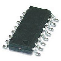
Pin Count
16
Package Type
SOIC N
Number Of Receivers
4
Number Of Drivers
4
Supply Current
23mA
Supply Voltage Range
3V To 3.6V
Driver Case Style
SOIC
No. Of Pins
16
Operating Temperature Range
-40°C To +85°C
Device Type
Differential Line Driver
Rohs Compliant
No
Data Rate Max
400Mbps
Lead Free Status / RoHS Status
Not Compliant
Available stocks
Company
Part Number
Manufacturer
Quantity
Price
Company:

Part Number:
DS90LV031BTM
Manufacturer:
NS
Quantity:
2
Company:
Part Number:
DS90LV031BTMX
Manufacturer:
NSC
Quantity:
6 613


www.national.com
of the ECL/PECL designs. LVDS requires about 80% less
current than similar PECL devices. AC specifications for the
driver are a tenfold improvement over other existing RS-422
drivers.
The TRI-STATE function allows the driver outputs to be dis-
abled, thus obtaining an even lower power state when the
transmission of data is not required.
The footprint of the DS90LV031B is the same as the industry
standard 26LS31 Quad Differential (RS-422) Driver and is a
step down replacement for the 5V DS90C031 Quad Driver.
POWER DECOUPLING RECOMMENDATIONS
Bypass capacitors must be used on power pins. High fre-
quency ceramic (surface mount is recommended) 0.1µF in
parallel with 0.01µF, in parallel with 0.001µF at the power
supply pin as well as scattered capacitors over the printed
circuit board. Multiple vias should be used to connect the de-
coupling capacitors to the power planes. A 10µF (35V) or
greater solid tantalum capacitor should be connected at the
power entry point on the printed circuit board.
PC BOARD CONSIDERATIONS
Use at least 4 PCB layers (top to bottom); LVDS signals,
ground, power, TTL signals.
Isolate TTL signals from LVDS signals, otherwise the TTL
may couple onto the LVDS lines. It is best to put TTL and
LVDS signals on different layers which are isolated by a pow-
er/ground plane(s).
Keep drivers and receivers as close to the (LVDS port side)
connectors as possible.
DIFFERENTIAL TRACES
Use controlled impedance traces which match the differential
impedance of your transmission medium (ie. cable) and ter-
mination resistor. Run the differential pair trace lines as close
together as possible as soon as they leave the IC (stubs
should be < 10mm long). This will help eliminate reflections
and ensure noise is coupled as common-mode. In fact, we
have seen that differential signals which are 1mm apart radi-
ate far less noise than traces 3mm apart since magnetic field
cancellation is much better with the closer traces. Plus, noise
induced on the differential lines is much more likely to appear
as common-mode which is rejected by the receiver.
Match electrical lengths between traces to reduce skew.
Skew between the signals of a pair means a phase difference
between signals which destroys the magnetic field cancella-
tion benefits of differential signals and EMI will result. (Note
the velocity of propagation, v = c/Er where c (the speed of
light) = 0.2997mm/ps or 0.0118 in/ps). Do not rely solely on
the autoroute function for differential traces. Carefully review
dimensions to match differential impedance and provide iso-
lation for the differential lines. Minimize the number or vias
and other discontinuities on the line.
Avoid 90° turns (these cause impedance discontinuities). Use
arcs or 45° bevels.
Within a pair of traces, the distance between the two traces
should be minimized to maintain common-mode rejection of
the receivers. On the printed circuit board, this distance
should remain constant to avoid discontinuities in differential
impedance. Minor violations at connection points are allow-
able.
TERMINATION
Use a resistor which best matches the differential impedance
or your transmission line. The resistor should be between
90Ω and 130Ω. Remember that the current mode outputs
6
need the termination resistor to generate the differential volt-
age. LVDS will not work without resistor termination. Typical-
ly, connect a single resistor across the pair at the receiver end.
Surface mount 1% to 2% resistors are best. PCB stubs, com-
ponent lead, and the distance from the termination to the
receiver inputs should be minimized. The distance between
the termination resistor and the receiver should be < 10mm
(12mm MAX).
PROBING LVDS TRANSMISSION LINES
Always use high impedance (> 100kΩ), low capacitance
(< 2pF) scope probes with a wide bandwidth (1GHz) scope.
Improper probing will give deceiving results.
CABLES AND CONNECTORS, GENERAL COMMENTS
When choosing cable and connectors for LVDS it is important
to remember:
Use controlled impedance media. The cables and connectors
you use should have a matched differential impedance of
about 100Ω. They should not introduce major impedance dis-
continuities.
Balanced cables (e.g. twisted pair) are usually better than
unbalanced cables (ribbon cable, simple coax.) for noise re-
duction and signal quality. Balanced cables tend to generate
less EMI due to field canceling effects and also tend to pick
up electromagnetic radiation a common-mode (not differential
mode) noise which is rejected by the receiver. For cable dis-
tances < 0.5M, most cables can be made to work effectively.
For distances 0.5M
pair cable works well, is readily available and relatively inex-
pensive.
FAIL-SAFE FEATURE
The LVDS receiver is a high gain, high speed device that am-
plifies a small differential signal (20mV) to CMOS logic levels.
Due to the high gain and tight threshold of the receiver, care
should be taken to prevent noise from appearing as a valid
signal.
The receiver's internal fail-safe circuitry is designed to source/
sink a small amount of current, providing fail-safe protection
(a stable known state of HIGH output voltage) for floating,
terminated or shorted receiver inputs.
1.
2.
3.
Open Input Pins. The DS90LV032A is a quad receiver
device, and if an application requires only 1, 2 or 3
receivers, the unused channel(s) inputs should be left
OPEN. Do not tie unused receiver inputs to ground or any
other voltages. The input is biased by internal high value
pull up and pull down resistors to set the output to a HIGH
state. This internal circuitry will guarantee a HIGH, stable
output state for open inputs.
Terminated Input. If the driver is disconnected (cable
unplugged), or if the driver is in a TRI-STATE or power-
off condition, the receiver output will again be in a HIGH
state, even with the end of cable 100Ω termination
resistor across the input pins. The unplugged cable can
become a floating antenna which can pick up noise. If the
cable picks up more than 10mV of differential noise, the
receiver may see the noise as a valid signal and switch.
To insure that any noise is seen as common-mode and
not differential, a balanced interconnect should be used.
Twisted pair cable will offer better balance than flat ribbon
cable.
Shorted Inputs. If a fault condition occurs that shorts
the receiver inputs together, thus resulting in a 0V
differential input voltage, the receiver output will remain
in a HIGH state. Shorted input fail-safe is not supported
≤
d
≤
10M, CAT 3 (category 3) twisted
Related parts for DS90LV031BTM
Image
Part Number
Description
Manufacturer
Datasheet
Request
R

Part Number:
Description:
National Semiconductor [8-Bit D/A Converter]
Manufacturer:
National Semiconductor
Datasheet:
Part Number:
Description:
National Semiconductor [Media Coprocessor]
Manufacturer:
National Semiconductor
Datasheet:
Part Number:
Description:
Digitally Controlled Tone and Volume Circuit with Stereo Audio Power Amplifier, Microphone Preamp Stage and National 3D Sound
Manufacturer:
National Semiconductor
Datasheet:
Part Number:
Description:
Digitally Controlled Tone and Volume Circuit with Stereo Audio Power Amplifier, Microphone Preamp Stage and National 3D Sound
Manufacturer:
National Semiconductor
Datasheet:
Part Number:
Description:
AC97 Rev 2 Codec with Sample Rate Conversion and National 3D Sound
Manufacturer:
National Semiconductor
Part Number:
Description:
Manufacturer:
National Semiconductor
Datasheet:
Part Number:
Description:
Manufacturer:
National Semiconductor
Datasheet:
Part Number:
Description:
General Purpose, Low Voltage, Low Power, Rail-to-Rail Output Operational Amplifiers
Manufacturer:
National Semiconductor
Datasheet:
Part Number:
Description:
8-bit 20 MSPS flash A/D converter.
Manufacturer:
National Semiconductor
Datasheet:
Part Number:
Description:
Low Noise Quad Operational Amplifier
Manufacturer:
National Semiconductor
Datasheet:
Part Number:
Description:
Quad Differential Line Receivers
Manufacturer:
National Semiconductor
Datasheet:
Part Number:
Description:
Quad High Speed Trapezoidal? Bus Transceiver
Manufacturer:
National Semiconductor
Datasheet:
Part Number:
Description:
Dual Line Receiver
Manufacturer:
National Semiconductor
Datasheet:
Part Number:
Description:
TTL to 10k ECL Level Translator with Latch
Manufacturer:
National Semiconductor
Datasheet: