DS90LV031BTM National Semiconductor, DS90LV031BTM Datasheet - Page 2
DS90LV031BTM
Manufacturer Part Number
DS90LV031BTM
Description
01C8071
Manufacturer
National Semiconductor
Datasheet
1.DS90LV031BTM.pdf
(10 pages)
Specifications of DS90LV031BTM
Number Of Elements
4
Input Type
CMOS/TTL
Operating Supply Voltage (typ)
3.3V
Differential Output Voltage
450mV
Propagation Delay Time
2ns
Power Dissipation
1.088W
Operating Temp Range
-40C to 85C
Operating Temperature Classification
Industrial
Mounting
Surface Mount
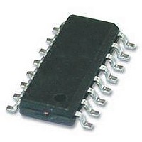
Pin Count
16
Package Type
SOIC N
Number Of Receivers
4
Number Of Drivers
4
Supply Current
23mA
Supply Voltage Range
3V To 3.6V
Driver Case Style
SOIC
No. Of Pins
16
Operating Temperature Range
-40°C To +85°C
Device Type
Differential Line Driver
Rohs Compliant
No
Data Rate Max
400Mbps
Lead Free Status / RoHS Status
Not Compliant
Available stocks
Company
Part Number
Manufacturer
Quantity
Price
Company:

Part Number:
DS90LV031BTM
Manufacturer:
NS
Quantity:
2
Company:
Part Number:
DS90LV031BTMX
Manufacturer:
NSC
Quantity:
6 613


www.national.com
V
ΔV
V
ΔV
V
V
V
V
I
I
V
I
I
I
I
I
I
I
IH
IL
OS
OSD
OFF
OZ
CC
CCL
CCZ
Symbol
OD1
OS
OH
OL
IH
IL
CL
Absolute Maximum Ratings
If Military/Aerospace specified devices are required,
please contact the National Semiconductor Sales Office/
Distributors for availability and specifications.
Electrical Characteristics
Over supply voltage and operating temperature ranges, unless otherwise specified. (Notes 3, 4, 5)
OD1
OS
Supply Voltage (V
Input Voltage (D
Enable Input Voltage (EN, EN*)
(Note 2)
Output Voltage (D
(Note 2)
Short Circuit Duration
Maximum Package Power Dissipation @ +25°C
Derate M Package
Storage Temperature Range
(D
M Package
OUT+
, D
Differential Output Voltage
Change in Magnitude of V
Complementary Output States
Offset Voltage
Change in Magnitude of V
Complementary Output States
Output Voltage High
Output Voltage Low
Input Voltage High
Input Voltage Low
Input Current
Input Current
Input Clamp Voltage
Output Short Circuit Current
Differential Output Short Circuit
Current
Power-off Leakage
Output TRI-STATE Current
No Load Supply Current Drivers
Enabled
Loaded Supply Current Drivers
Enabled
No Load Supply Current Drivers
Disabled
OUT−
IN
)
)(Note 2)
CC
OUT+
)
Parameter
, D
OUT−
)
8.5 mW/°C above +25°C
OD1
OS
−0.6V to (V
−0.6V to (V
for
for
−65°C to +150°C
−0.6V to +3.9V
−0.3V to +4V
(Note 1)
Continuous
R
V
V
I
ENABLED, (Note 11)
D
D
ENABLED, V
V
V
EN = 0.8V and EN* = 2.0V
V
D
R
D
D
EN = GND, EN* = V
CL
CC
CC
1088 mW
IN
IN
OUT
CC
OUT
L
IN
IN
IN
L
IN
IN
= 100Ω (Figure 1)
= 100Ω All Channels,
= −18 mA
= V
= GND or 0.4V
+ 0.3V)
+ 0.3V)
= V
= GND, D
= V
= V
= V
= 0V or Open
= 0V or 3.6V,
= 0V or V
CC
CC
CC
CC
CC
, D
or 2.5V
or GND
or GND (all inputs)
or GND,
Conditions
OUT+
OD
OUT−
CC
2
= 0V (Note 11)
= 0V or
= 0V
Recommended Operating
Conditions
CC
Lead Temperature Range
Maximum Junction Temperature
ESD Rating
Supply Voltage (V
Operating Free Air
Temperature (T
Soldering (4 sec.)
(HBM, 1.5 kΩ, 100 pF)
(EIAJ, 0 Ω, 200 pF)
(CDM)
D
A
D
D
D
D
)
IN
EN*
V
Pin
CC
OUT−
OUT+
OUT−
OUT+
, EN,
CC
)
1.125
GND
0.90
−1.5
Min
250
−10
−10
−20
−10
+3.0
2.0
Min
−40
+3.3
Typ
+25
1.25
1.38
1.03
−0.8
−6.0
−6.0
Typ
350
5.0
2.6
±1
±1
±1
±1
23
4
5
Max
+3.6
+85
1.375
−9.0
−9.0
Max
V
450
+10
+10
+20
+10
1.6
0.8
8.0
6.0
35
25
30
CC
≥
≥
+260°C
+150°C
1250 V
Units
≥
500 V
°C
V
7 kV
Units
|mV|
|mV|
mV
mA
mA
mA
mA
mA
μA
μA
μA
μA
V
V
V
V
V
V
Related parts for DS90LV031BTM
Image
Part Number
Description
Manufacturer
Datasheet
Request
R

Part Number:
Description:
National Semiconductor [8-Bit D/A Converter]
Manufacturer:
National Semiconductor
Datasheet:
Part Number:
Description:
National Semiconductor [Media Coprocessor]
Manufacturer:
National Semiconductor
Datasheet:
Part Number:
Description:
Digitally Controlled Tone and Volume Circuit with Stereo Audio Power Amplifier, Microphone Preamp Stage and National 3D Sound
Manufacturer:
National Semiconductor
Datasheet:
Part Number:
Description:
Digitally Controlled Tone and Volume Circuit with Stereo Audio Power Amplifier, Microphone Preamp Stage and National 3D Sound
Manufacturer:
National Semiconductor
Datasheet:
Part Number:
Description:
AC97 Rev 2 Codec with Sample Rate Conversion and National 3D Sound
Manufacturer:
National Semiconductor
Part Number:
Description:
Manufacturer:
National Semiconductor
Datasheet:
Part Number:
Description:
Manufacturer:
National Semiconductor
Datasheet:
Part Number:
Description:
General Purpose, Low Voltage, Low Power, Rail-to-Rail Output Operational Amplifiers
Manufacturer:
National Semiconductor
Datasheet:
Part Number:
Description:
8-bit 20 MSPS flash A/D converter.
Manufacturer:
National Semiconductor
Datasheet:
Part Number:
Description:
Low Noise Quad Operational Amplifier
Manufacturer:
National Semiconductor
Datasheet:
Part Number:
Description:
Quad Differential Line Receivers
Manufacturer:
National Semiconductor
Datasheet:
Part Number:
Description:
Quad High Speed Trapezoidal? Bus Transceiver
Manufacturer:
National Semiconductor
Datasheet:
Part Number:
Description:
Dual Line Receiver
Manufacturer:
National Semiconductor
Datasheet:
Part Number:
Description:
TTL to 10k ECL Level Translator with Latch
Manufacturer:
National Semiconductor
Datasheet: