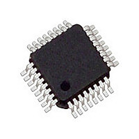
MC34910G5AC Freescale, MC34910G5AC Datasheet - Page 24

MC34910G5AC
Manufacturer Part Number
MC34910G5AC
Description
Manufacturer
Freescale
Datasheet
1.MC34910G5AC.pdf
(90 pages)
Specifications of MC34910G5AC
Turn Off Delay Time
10us
Number Of Drivers
2
Operating Temperature (min)
-40C
Lead Free Status / RoHS Status
Compliant
Available stocks
Company
Part Number
Manufacturer
Quantity
Price
Company:
Part Number:
MC34910G5AC
Manufacturer:
Freescale Semiconductor
Quantity:
10 000
Company:
Part Number:
MC34910G5ACR2
Manufacturer:
Freescale Semiconductor
Quantity:
10 000
integrated and cost-effective solution for automotive and
industrial applications. For automotive body electronics, the
33910 is well suited to perform keypad applications via the
LIN bus.
high side outputs. Other ports are also provided, which
graphic representation of the various pins referred to in the
following paragraphs. Also, see
description of the pin locations in the package.
RECEIVER OUTPUT PIN (RXD)
the LIN interface and reports the state of the bus voltage:
RXD Low when LIN bus is dominant, RXD High when LIN bus
is recessive.
TRANSMITTER INPUT PIN (TXD)
the LIN interface and controls the state of the bus output
(dominant when TXD is Low, recessive when TXD is High).
case the input is left floating.
LIN BUS PIN (LIN)
receiver. It is suited for automotive bus systems and is
compliant to the LIN bus specification 2.0, 2.1, and SAE
J2602-2.
Table 6, Operating Modes
SERIAL DATA CLOCK PIN (SCLK)
on the positive transition of the SCLK. MOSI is sampled on
the negative edge of the SCLK.
24
33910
FUNCTIONAL DESCRIPTION
INTRODUCTION
The 33910 was designed and developed as a highly
Power switches are provided on the device configured as
See
The RXD pin is a digital output. It is the receiver output of
The TXD pin is a digital input. It is the transmitter input of
This pin has an internal pull-up to force recessive state in
The LIN pin represents the single-wire bus transmitter and
The LIN interface is only active during Normal mode. See
The SCLK pin is the SPI clock input. MISO data changes
Figure 1, 33910 Simplified Application
Overview.
Pin Connections
FUNCTIONAL DESCRIPTION
FUNCTIONAL PIN DESCRIPTION
Diagram, for a
for a
INTRODUCTION
include a Hall Sensor port supply, and one wake-up capable
pin. An internal voltage regulator provides power to a MCU
device.
communicates using a single wire. This enables this device
to be compatible with 3-wire bus systems, where one wire is
used for communication, one for battery, and one for ground.
MASTER OUT SLAVE IN PIN (MOSI)
data input is sampled on the negative edge of SCLK.
MASTER IN SLAVE OUT PIN (MISO)
digital tri-state output used to shift serial data to the
microcontroller. Data on this output pin changes on the
positive edge of the SCLK. When CS is High, this pin will
remain in the high-impedance state.
CHIP SELECT PIN (CS)
a valid SPI communication and allow for several devices to
be connected in the same SPI bus without contention. A
rising edge on CS signals the end of the transmission and the
moment the data shifted in is latched. A valid transmission
must consist of 8 bits only.
pin will generate a wake-up condition for the 33910.
ANALOG MULTIPLEXER PIN (ADOUT0)
the MCU A/D converter to read the several inputs of the
Analog Multiplexer, including the VSENSE and L1 input
voltages, and the internal junction temperature.
PWM INPUT CONTROL PIN (PWMIN)
Normal Request and Normal mode.
operation to the High Side Control Register (HSCR).
Also included in this device is a LIN physical layer, which
The MOSI digital pin receives SPI data from the MCU. This
The MISO pin sends data to an SPI-enabled MCU. It is a
CS is an active low digital input. It must remain low during
While in STOP mode, a low-to-high level transition on this
The ADOUT0 pin can be configured via the SPI to allow
This digital input can control the high sides drivers in
To enable PWM control, the MCU must perform a write
This pin has an internal 20 μA current pull-up.
Analog Integrated Circuit Device Data
Freescale Semiconductor


