LF198H/883 National Semiconductor, LF198H/883 Datasheet
LF198H/883
Specifications of LF198H/883
Available stocks


Related parts for LF198H/883

LF198H/883 Summary of contents
Page 1
... The overall design guarantees no feed-through from input to output in the hold mode, even for input signals equal to the supply voltages. Ordering Information NSC Part Number JAN Part Number LF198H/883 5962–8760801GA LF198WG-QMLV 5962–8760801VZA LF198WG/883 5962–8760801QZA ...
Page 2
Typical Connection and Performance Curve Functional Diagram www.national.com Acquisition Time 20122232 2 20122216 20122201 ...
Page 3
Absolute Maximum Ratings Supply Voltage Power Dissipation (Package Limitation) (Note 2) Operating Ambient Temperature Range Maximum Junction Temperature (T Jmax Input Voltage Logic To Logic Reference Differential Voltage (Note 3) Output Short Circuit Duration Hold Capacitor Short Circuit Duration Lead ...
Page 4
Electrical Characteristics The following specifications apply unless otherwise specified. V erence Pin = 0V, Logic Pin = 4V Symbol Parameter I + Positive Supply Current Negative Supply Current CC V Input Offset Voltage OS I Input Bias ...
Page 5
Electrical Characteristics The following specifications apply unless otherwise specified. V erence Pin = 0V, Logic Pin = 4V Symbol Parameter V Hold Step HS A Gain Error E Z Input Impedance I Z Output Impedance O I Capacitor Charging Current ...
Page 6
Electrical Characteristics The following specifications apply unless otherwise specified. V erence Pin = 0V, Logic Pin = 4V Symbol Parameter V 2nd Stage (2nd Stg) AC Parameters The following specifcations apply unless otherwise specified. V ence Pin ...
Page 7
Typical Performance Characteristics Aperture Time (Note 6) Dynamic Sampling Error Hold Step Error in Hold Capacitor 20122217 20122219 20122221 7 Dielectric Absorption 20122218 Output Droop Rate 20122220 “Hold” Settling Time (Note 6) 20122222 www.national.com ...
Page 8
Typical Performance Characteristics Leakage Current into Hold Capacitor Gain Error Output Short Circuit Current www.national.com (Continued) Phase and Gain (Input to Output, Small Signal) 20122223 Power Supply Rejection 20122225 20122227 Note 9: See Definition 8 20122224 20122226 Output Noise 20122228 ...
Page 9
Typical Performance Characteristics Input Bias Current Hold Step vs Input Voltage Output Transient at Start of Hold Mode (Continued) Feedthrough Rejection Ratio 20122229 Output Transient at Start 20122231 20122213 9 (Hold Mode) 20122230 of Sample Mode 20122212 www.national.com ...
Page 10
Logic Input Configurations TTL & CMOS 3V ≤ V (Hi State) ≤ 7V LOGIC Threshold = 1.4V CMOS 7V ≤ V (Hi State) ≤ 15V LOGIC + Threshold = 0 1.4V Op Amp Drive Threshold ≈ +4V ...
Page 11
Application Hints HOLD CAPACITOR Hold step, acquisition time, and droop rate are the major trade-offs in the selection of a hold capacitor value. Size and cost may also become important for larger values. Use of the curves included with this ...
Page 12
Typical Applications X1000 Sample & Hold *For lower gains, the LM108 must be frequency compensated Ramp Generator with Variable Reset Level www.national.com Sample and Difference Circuit (Output Follows Input in Hold Mode) + ∆ (HOLD MODE) OUT ...
Page 13
Typical Applications (Continued) Output Holds at Average of Sampled Input Reset Stabilized Amplifier (Gain of 1000) 20122246 Fast Acquisition, Low Droop Sample & Hold 20122249 13 Increased Slew Current 20122247 20122250 www.national.com ...
Page 14
Typical Applications Synchronous Correlator for Recovering Signals Below Noise Level DC & AC Zeroing www.national.com (Continued) 20122252 A B ± ± Gain 1 0.02% 1 0.2% Ω kΩ MHz . 400 kHz BW ...
Page 15
Typical Applications (Continued) Differential Hold Definition of Terms Hold Step: The voltage step at the output of the sample and hold when switching from sample mode to hold mode with a steady (dc) analog input voltage. Logic swing is 5V. ...
Page 16
Revision History Section Date Revision Released 02/25/05 A New release, Corporate format www.national.com Section Originator L. Lytle 1 MDS converted to corp. datasheet format. MNLF198–X Rev 3B0 MDS to be archived. Change has been made to Electrical Section, Parameter I ...
Page 17
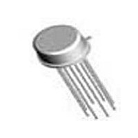
Physical Dimensions inches (millimeters) unless otherwise noted Metal Can Package (H) NS Package Number H08C 14 LD Ceramic SOIC (WG) NS Package Number WG14A 17 www.national.com ...
Page 18
... BANNED SUBSTANCE COMPLIANCE National Semiconductor manufactures products and uses packing materials that meet the provisions of the Customer Products Stewardship Specification (CSP-9-111C2) and the Banned Substances and Materials of Interest Specification (CSP-9-111S2) and contain no ‘‘Banned Substances’’ as defined in CSP-9-111S2. ...