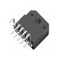
LM3886TF National Semiconductor, LM3886TF Datasheet - Page 3

LM3886TF
Manufacturer Part Number
LM3886TF
Description
92F299
Manufacturer
National Semiconductor
Datasheet
1.LM3886TF.pdf
(24 pages)
Specifications of LM3886TF
Operational Class
Class-AB
Audio Amplifier Output Configuration
1-Channel Mono
Output Power (typ)
68x1@4OhmW
Audio Amplifier Function
Speaker
Input Offset Voltage
10@±28VmV
Input Bias Current
1uA
Total Harmonic Distortion
0.03@4Ohm@60W%
Single Supply Voltage (typ)
18V
Dual Supply Voltage (typ)
±12/±15/±18/±24V
Power Supply Requirement
Single/Dual
Power Dissipation
125W
Unity Gain Bandwidth Product (typ)
8MHz
Rail/rail I/o Type
No
Power Supply Rejection Ratio
120dB
Single Supply Voltage (min)
20V
Single Supply Voltage (max)
84V
Dual Supply Voltage (min)
±10V
Dual Supply Voltage (max)
±42V
Operating Temp Range
-20C to 85C
Operating Temperature Classification
Commercial
Mounting
Through Hole
Pin Count
11 +Tab
Package Type
TO-220
Amplifier Class
AB
No. Of Channels
1
Output Power
68W
Supply Voltage Range
20V To 84V
Load Impedance
4ohm
Operating Temperature Range
-20°C To +85°C
Amplifier Case Style
TO-220
Rohs Compliant
No
Lead Free Status / RoHS Status
Not Compliant
Available stocks
Company
Part Number
Manufacturer
Quantity
Price
Part Number:
LM3886TF
Manufacturer:
CN/如韵
Quantity:
20 000
Company:
Part Number:
LM3886TF/NOPB
Manufacturer:
AVX
Quantity:
40 000
Part Number:
LM3886TF/NOPB
Manufacturer:
TI/德州仪器
Quantity:
20 000
|V
A
P
Peak P
THD + N
SR (Note 4) Slew Rate (Note 13)
I
V
(Note 3)
I
I
I
V
(Note 3)
PSRR
(Note 3)
+
B
OS
o
M
O
OS
od
Symbol
+
Absolute Maximum Ratings
If Military/Aerospace specified devices are required, please contact the National Semiconductor Sales Office/
Distributors for availability and specifications.
Operating Ratings
Electrical Characteristics
(Note 4)
Temperature Range
| + |V
Supply Voltage |V
Supply Voltage |V
Common Mode Input Voltage
Differential Input Voltage (Note
16)
Output Current
Power Dissipation (Note 7)
The following specifications apply for V
apply for T
(Note 4) Output Power (Continuous Average)
T
(No Signal)
(Input Signal)
MIN
O
−
|
≤ T
Power Supply Voltage (Note 14)
Mute Attenuation
Instantaneous Peak Output Power
Total Harmonic Distortion Plus Noise
Total Quiescent Power Supply Current V
Input Offset Voltage
Input Bias Current
Input Offset Current
Output Current Limit
Output Dropout Voltage (Note 15)
Power Supply Rejection Ratio
A
A
≤ T
= 25˚C.
MAX
+
+
|+|V
|+|V
−
−
|
|
Parameter
(Notes 5, 6)
+
Internally Limited
|V
= +28V, V
(Notes 5, 6)
+
(V
| + |V
−20˚C ≤ T
+
(Notes 6, 5)
or V
−
| ≤ 80V
V
Pin 8 Open or at 0V, Mute: On
Current out of Pin 8
Mute: Off
THD + N = 0.1% (max)
f = 1 kHz; f = 20 kHz
|V
|V
|V
60W, R
30W, R
20 Hz ≤ f ≤ 20 kHz
A
V
V
V
V
|V
|V
|V
V
V
V
V
−
−
+85˚C
125W
) and
pin7
V
IN
CM
CM
CM
CM
+
CM
+
CM
= −28V, I
+
+
+
+
+
O
94V
84V
60V
| = |V
| = |V
| = |V
| = |V
–V
= 40V to 20V, V
= 40V, V
= 26 dB
A
–V
= 2.0Vp-p, t
= 0V, V
= 0V, I
= 0V, I
= 0V, I
= 0V, I
= 0V, I
≤
− V
O
−
|, V
|, V
L
L
−
−
−
−
−
= 4Ω,
= 8Ω,
| = 28V, R
| = 28V, R
| = 35V, R
| = 20V, t
≥ 9V
+
−
3
MUTE
o
o
o
o
o
−
o
= 28V, I
= −28V, I
= 0 mA
= 0 mA
= 0 mA
= 0 mA
= 0 mA
= −40V to −20V,
= 0V, I
Supply Voltage |V
RISE
ESD Susceptibility (Note 8)
Junction Temperature (Note 9)
Soldering Information
Storage Temperature
Thermal Resistance
Conditions
= −0.5 mA with R
T Package (10 seconds)
θ
θ
ON
JC
JA
−
L
L
L
o
>
= 2 ns
o
= −40V,
= 4Ω
= 8Ω
= 8Ω
o
= 10 ms, V
= +100 mA
= 0A
0.5 mA,
= −100 mA
O
+
L
| + |V
= 0V
= 4Ω unless otherwise specified. Limits
−
|
(Note 10)
Typical
0.03
0.03
0.01
11.5
115
135
120
105
0.2
1.6
2.5
18
68
38
50
19
50
1
LM3886
(Note 11)
−40˚C to +150˚C
Limit
0.2
2.0
3.0
20
84
80
60
30
85
10
85
85
8
1
7
20V to 84V
www.national.com
43˚C/W
3000V
1˚C/W
150˚C
260˚C
V/µs (min)
mA (max)
mV (max)
µA (max)
µA (max)
dB (min)
dB (min)
dB (min)
(Limits)
V (max)
W (min)
W (min)
V (max)
V (max)
V (min)
A (min)
Units
W
W
%
%


