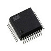
SAA7128H/V1 NXP Semiconductors, SAA7128H/V1 Datasheet - Page 19

SAA7128H/V1
Manufacturer Part Number
SAA7128H/V1
Description
Manufacturer
NXP Semiconductors
Datasheet
1.SAA7128HV1.pdf
(55 pages)
Specifications of SAA7128H/V1
Adc/dac Resolution
10b
Screening Level
Commercial
Package Type
PQFP
Pin Count
44
Lead Free Status / RoHS Status
Compliant
Philips Semiconductors
9397 750 14325
Product data sheet
Table 11:
Table 12:
Table 13:
Table 14:
Table 15:
Bit
7
6
5
4
3
2
1
0
Bit
7
6
5
4
3
2
1
0
Bit
7 to 0
Bit
7 to 0
Bit
7
6
5
4
Subaddress 28h
Subaddress 29h
Subaddress 2Ah
Subaddress 2Bh
Subaddress 2Ch
Symbol
DECCOL
DECFIS
BS5
BS4
BS3
BS2
BS1
BS0
Symbol
-
-
BE5
BE4
BE3
BE2
BE1
BE0
Symbol
CG[07:00] LSB of the byte is encoded immediately after run-in, the MSB of the byte
Symbol
CG[15:08] second byte; the MSB of the byte has to carry the CRCC bit, in
Symbol
CGEN
-
-
-
Rev. 03 — 9 December 2004
Description
0 = disable color detection bit of RTCI input,
1 = enable color detection bit of RTCI input; bit RTCE must be set to
logic 1, see
0 = field sequence as FISE in subaddress 61,
1 = field sequence as FISE bit in RTCI input; bit RTCE must be set to
logic 1, see
starting point of burst in clock cycles:
Description
these 2 bits are reserved; each must be set to logic 0
ending point of burst in clock cycles:
Description
has to carry the CRCC bit, in accordance with the definition of copy
generation management system encoding format
Description
accordance with the definition of copy generation management system
encoding format
Description
0 = copy generation data output is disabled; default state after reset,
1 = copy generation data output is enabled.
these 3 bits are reserved; each must be set to logic 0
PAL: BS[5:0] = 33 (21h); default value after reset
NTSC: BS[5:0] = 25 (19h).
PAL: BE[5:0] = 29 (1Dh); default value after reset
NTSC: BE[5:0] = 29 (1Dh).
Figure 22
Figure 22
SAA7128H; SAA7129H
© Koninklijke Philips Electronics N.V. 2004. All rights reserved.
Digital video encoder
19 of 55


