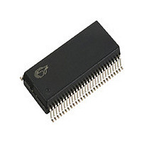
CY7C68000-56PVC Cypress Semiconductor Corp, CY7C68000-56PVC Datasheet - Page 13

CY7C68000-56PVC
Manufacturer Part Number
CY7C68000-56PVC
Description
Manufacturer
Cypress Semiconductor Corp
Datasheet
1.CY7C68000-56PVC.pdf
(14 pages)
Specifications of CY7C68000-56PVC
Number Of Transceivers
1
Power Supply Requirement
Single
Operating Supply Voltage (typ)
3.3V
Operating Temperature Classification
Commercial
Operating Supply Voltage (max)
3.6V
Operating Supply Voltage (min)
3V
Dual Supply Voltage (typ)
Not RequiredV
Dual Supply Voltage (max)
Not RequiredV
Dual Supply Voltage (min)
Not RequiredV
Mounting
Surface Mount
Operating Temperature (max)
70C
Operating Temperature (min)
0C
Lead Free Status / RoHS Status
Not Compliant
Available stocks
Company
Part Number
Manufacturer
Quantity
Price
Company:
Part Number:
CY7C68000-56PVC
Manufacturer:
INFINEON
Quantity:
67
Company:
Part Number:
CY7C68000-56PVC
Manufacturer:
CY
Quantity:
129
Company:
Part Number:
CY7C68000-56PVCT
Manufacturer:
EPCOS
Quantity:
4 000
13.0
Package Design Notes
Electrical contact of the part to the Printed Circuit Board (PCB)
is made by soldering the leads on the bottom surface of the
package to the PCB. Hence, special attention is required to the
heat transfer area below the package to provide a good ther-
mal bond to the circuit board. A Copper (Cu) fill is to be de-
signed into the PCB as a thermal pad under the package. Heat
is transferred from the TX2 through the device’s metal paddle
on the bottom side of the package. Heat from here, is conduct-
ed to the PCB at the thermal pad. It is then conducted from the
thermal pad to the PCB inner ground plane by an array of via.
A via is a plated through hole in the PCB with a finished diam-
eter of 13 mil. The QFN’s metal die paddle must be soldered
to the PCB’s thermal pad. Solder mask is placed on the board
top side over each via to resist solder flow into the via. The
Figure 13-2 is a plot of the solder mask pattern image of the assembly (darker areas indicate solder).
EZ-USB TX2 is a trademark of Cypress Semiconductor Corporation. All product and company names mentioned in this document
are the trademarks of their respective holders.
Document #: 38-08016 Rev. *H
© Cypress Semiconductor Corporation, 2006. The information contained herein is subject to change without notice. Cypress Semiconductor Corporation assumes no responsibility for the use
of any circuitry other than circuitry embodied in a Cypress product. Nor does it convey or imply any license under patent or other rights. Cypress products are not warranted nor intended to be
used for medical, life support, life saving, critical control or safety applications, unless pursuant to an express written agreement with Cypress. Furthermore, Cypress does not authorize its
products for use as critical components in life-support systems where a malfunction or failure may reasonably be expected to result in significant injury to the user. The inclusion of Cypress
products in life-support systems application implies that the manufacturer assumes all risk of such use and in doing so indemnifies Cypress against all charges.
Quad Flat Package No Leads (QFN)
Via hole for thermally connecting the
QFN to the circuit board ground plane.
Figure 13-1. Crosssection of the Area Underneath the QFN Package
PCB Material
Figure 13-2. Plot of the Solder Mask (White Area)
Cu Fill
Solder Mask
0.013” dia
0.017” dia
mask on the top side also minimizes outgassing during the
solder reflow process.
For further information on this package design please refer to
the application note “Surface Mount Assembly of AMKOR’s
MicroLeadFrame (MLF) Technology.” This application note
can be downloaded from AMKOR’s web site from the following
URL http://www.amkor.com/products/notes_papers/MLFApp
Note.pdf. The application note provides detailed information
on board mounting guidelines, soldering flow, rework process,
etc.
Figure 13-1 below displays a cross-sectional area underneath
the package. The cross section is of only one via. The solder
paste template needs to be designed to allow at least 50%
solder coverage. The thickness of the solder paste template
should be 5 mil. Cypress recommends that ’No Clean’, type 3
solder paste is used for mounting the part. Nitrogen purge is
recommended during reflow.
This figure only shows the top three layers of the
circuit board: Top Solder, PCB Dielectric, and
the Ground Plane
Cu Fill
PCB Material
CY7C68000
Page 13 of 14


