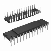
STK12C68-5K35M Cypress Semiconductor Corp, STK12C68-5K35M Datasheet - Page 7

STK12C68-5K35M
Manufacturer Part Number
STK12C68-5K35M
Description
STK12C68-5K35M
Manufacturer
Cypress Semiconductor Corp
Type
NVSRAMr
Datasheet
1.STK12C68-5C55M.pdf
(18 pages)
Specifications of STK12C68-5K35M
Format - Memory
RAM
Memory Type
NVSRAM (Non-Volatile SRAM)
Memory Size
64K (8K x 8)
Speed
35ns
Interface
Parallel
Voltage - Supply
4.5 V ~ 5.5 V
Operating Temperature
-55°C ~ 125°C
Package / Case
28-CDIP (0.300", 7.62mm)
Word Size
8b
Organization
8Kx8
Density
64Kb
Interface Type
Parallel
Access Time (max)
35ns
Operating Supply Voltage (typ)
5V
Operating Temperature Classification
Military
Operating Supply Voltage (max)
5.5V
Operating Supply Voltage (min)
4.5V
Operating Temp Range
-55C to 125C
Pin Count
28
Mounting
Through Hole
Supply Current
75mA
Lead Free Status / RoHS Status
Contains lead / RoHS non-compliant
Lead Free Status / RoHS Status
Contains lead / RoHS non-compliant
Maximum Ratings
Exceeding maximum ratings may shorten the useful life of the
device. These user guidelines are not tested.
Storage Temperature ................................. –65°C to +150°C
Temperature under Bias ............................. –55°C to +125°C
Voltage on Input Relative to GND.....................–0.5V to 7.0V
Voltage on Input Relative to Vss............ –0.6V to V
DC Electrical Characteristics
Over the operating range (V
Document Number: 001-51026 Rev. **
Parameter
I
I
I
I
I
I
I
I
V
V
V
V
V
V
Notes
CC1
CC2
CC3
CC4
SB1
SB2
IX
OZ
4. V
5. CE > V
IH
IL
OH
OL
BL
CAP
[5]
[5]
CC
reference levels throughout this data sheet refer to VCC if that is where the power supply connection is made, or V
IH
does not produce standby current levels until any nonvolatile cycle in progress has timed out.
Average V
Average V
during STORE
Average V
t
Typical
Average V
during AutoStore Cycle
V
(Standby, Cycling TTL
Input Levels)
V
Input Leakage Current V
Off State Output
Leakage Current
Input HIGH Voltage
Input LOW Voltage
Output HIGH Voltage
Output LOW Voltage
Logic ‘0’ Voltage on
HSB Output
Storage Capacitor
RC
CC
CC
= 200 ns, 5V, 25°C
Standby Current
Standby Current
Description
CC
CC
CC
CAP
Current at
Current
Current
Current
CC
= 4.5V to 5.5V)
t
t
Dependent on output loading and cycle rate. Values
obtained without output loads.
I
All Inputs Do Not Care, V
Average current for duration t
WE > (V
Dependent on output loading and cycle rate. Values
obtained without output loads.
All Inputs Do Not Care, V
Average current for duration t
t
t
CE > (V
Standby current level after nonvolatile cycle is complete.
Inputs are static. f = 0 MHz.
V
I
I
I
Between Vcap pin and Vss, 6V rated. 68 µF +20% nom.
RC
RC
OUT
RC
RC
OUT
OUT
OUT
CC
CC
= 35 ns
= 55 ns
= 35 ns, CE > V
= 55 ns, CE > V
= Max, V
= Max, V
= 0 mA.
= –4 mA
= 8 mA
= 3 mA
CC
CC
[4]
– 0.2V). All others V
– 0.2V). All other inputs cycling.
CC
SS
SS
< V
< V
+ 0.5V
IH
IH
IN
IN
Test Conditions
< V
< V
CC
CC
CC
CC
= Max
= Max
, CE or OE > V
STORE
STORE
IN
Voltage on DQ
Power Dissipation.......................................................... 1.0W
DC output Current (1 output at a time, 1s duration) .... 15 mA
Operating Range
Military
< 0.2V or > (V
Range
IH
STK12C68-5 (SMD5962-94599)
0-7
or WE < V
CC
Ambient Temperature
or HSB .......................–0.5V to Vcc + 0.5V
– 0.2V).
-55°C to +125°C
IL
V
CAP
SS
Min
2.2
2.4
54
-1
-5
if VCC is connected to ground.
– 0.5
V
CC
Max
260
2.5
0.8
0.4
0.4
75
55
10
24
19
+1
+5
3
2
+ 0.5
4.5V to 5.5V
Page 7 of 18
V
CC
Unit
mA
mA
mA
mA
mA
mA
mA
mA
μA
μA
µF
V
V
V
V
V
[+] Feedback


