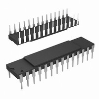
STK11C68-5K45M Cypress Semiconductor Corp, STK11C68-5K45M Datasheet

STK11C68-5K45M
Specifications of STK11C68-5K45M
Available stocks
Related parts for STK11C68-5K45M
STK11C68-5K45M Summary of contents
Page 1
... Document Number: 001-51001 Rev. *A STK11C68-5 (SMD5962-92324) 64 Kbit ( SoftStore nvSRAM Functional Description The Cypress STK11C68 fast static RAM with a nonvolatile element in each memory cell. The embedded nonvolatile elements incorporate QuantumTrap technology to produce the world’s most reliable nonvolatile memory. The SRAM provides unlimited read and write cycles, while independent nonvolatile data resides in the highly reliable QuantumTrap cell ...
Page 2
... Deasserting OE HIGH causes the I/O pins to tristate. V Ground Ground for the Device. The device is connected to ground of the system Power Supply Power Supply Inputs to the Device. CC Document Number: 001-51001 Rev. *A STK11C68-5 (SMD5962-92324) Figure 2. Pin Diagram - 28-Pin LLC Description Page [+] Feedback ...
Page 3
... RECALL request is latched. When V RESET once again exceeds the sense voltage of V cycle is automatically initiated and takes t If the STK11C68 Write state at the end of power up RECALL, the SRAM data is corrupted. To help avoid this situation Kohm resistor is connected either between WE and system V ...
Page 4
... CMOS and TTL input levels (commercial temperature range, VCC = 5.5V, 100% duty cycle on chip enable). Only standby current is drawn when the chip is disabled. The overall average current drawn by the STK11C68-5 depends on the following items: ■ Duty cycle of chip enable ■ ...
Page 5
... IH 3. These parameters are guaranteed by design and are not tested. Document Number: 001-51001 Rev. *A STK11C68-5 (SMD5962-92324) Voltage on DQ Power Dissipation ......................................................... 1.0W DC Output Current (1 output at a time, 1s duration).... 15 mA ...
Page 6
... AC Test Conditions Input Pulse Levels .................................................... Input Rise and Fall Times (10% to 90%) ...................... <5 ns Input and Output Timing Reference Levels .................... 1.5V Document Number: 001-51001 Rev. *A STK11C68-5 (SMD5962-92324) [3] Test Conditions Test conditions follow standard test methods and proce- dures for measuring thermal impedance, per EIA / JESD51 ...
Page 7
... Figure 6. SRAM Read Cycle 1: Address Controlled Figure 7. SRAM Read Cycle 2: CE and OE Controlled Notes 4. WE must be High during SRAM Read cycles. 5. I/O state assumes CE and OE < V and WE > Measured ± 200 mV from steady state output voltage. Document Number: 001-51001 Rev. *A STK11C68-5 (SMD5962-92324 Min Max ...
Page 8
... PREVIOUS DATA DATA OUT Figure 9. SRAM Write Cycle 2: CE and OE Controlled ADDRESS DATA IN DATA OUT Notes Low when CE goes Low, the outputs remain in the high impedance state must be greater than V during address transitions. IH Document Number: 001-51001 Rev. *A STK11C68-5 (SMD5962-92324 Description Min Max ...
Page 9
... STORE INHIBIT POWER-UP RECALL t HRECALL DQ (DATA OUT) POWER-UP RECALL Notes 9. t starts from the time V rises above V HRECALL CC Document Number: 001-51001 Rev. *A STK11C68-5 (SMD5962-92324) Description BROWN OUT BROWN OUT STORE INHIBIT STORE INHIBIT NO RECALL NO RECALL (V DID NOT GO (V DID NOT BELOW V ...
Page 10
... SCE CE t HACE OE DATA VALID DQ (DATA) Notes 10. The software sequence is clocked on the falling edge of CE without involving OE (double clocking aborts the sequence). 11. The six consecutive addresses must be read in the order listed in Document Number: 001-51001 Rev. *A STK11C68-5 (SMD5962-92324) [10, 11 Description Min Max ...
Page 11
... Part Numbering Nomenclature STK11C68 - SMD5962-92324 Document Number: 001-51001 Rev. *A STK11C68-5 (SMD5962-92324) Temperature Range Military (-55 to 125°C) Package Ceramic 28-pin 300 mil DIP (gold lead finish Ceramic 28-pin 300 mil DIP (Solder dip finish Ceramic 28-pin LLC Retention / Endurance Military (10 years or 10 ...
Page 12
... Ordering Information Speed (ns) Ordering Code 35 STK11C68-5C35M STK11C68-5K35M STK11C68-5L35M 45 STK11C68-5C45M STK11C68-5K45M STK11C68-5L45M 55 STK11C68-5C55M STK11C68-5K55M STK11C68-5L55M This table contains Final information. Contact your local Cypress sales representative for availability of these parts. Document Number: 001-51001 Rev. *A STK11C68-5 (SMD5962-92324) Package Diagram Package Type 001-51695 28-Pin CDIP (300 mil) ...
Page 13
... Package Diagrams Figure 12. 28-Pin (300-Mil) Side Braze DIL (001-51695) Document Number: 001-51001 Rev. *A STK11C68-5 (SMD5962-92324) 001-51695 ** Page [+] Feedback ...
Page 14
... Package Diagrams (continued) 1. ALL DIMENSION ARE IN INCHES AND MILLIMETERS [MIN/MAX] 2. JEDEC 95 OUTLINE# MO-041 3. PACKAGE WEIGHT : TBD Document Number: 001-51001 Rev. *A STK11C68-5 (SMD5962-92324) Figure 13. 28-Pad (350-Mil) LCC (001-51696) 001-51696 ** Page [+] Feedback ...
Page 15
... AutoStore and QuantumTrap are registered trademarks of Cypress Semiconductor Corporation. All products and company names mentioned in this document may be the trademarks of their respective holders. STK11C68-5 (SMD5962-92324) Submission Date 03/02/09 New data sheet 04/07/2009 Added part numbers: STK11C68-5K45M and STK11C68-5K55M PSoC Solutions psoc.cypress.com General clocks.cypress.com Low Power/Low Voltage Precision Analog LCD Drive image ...


