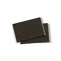
S29JL032H70TFI420 Spansion Inc., S29JL032H70TFI420 Datasheet - Page 26

S29JL032H70TFI420
Manufacturer Part Number
S29JL032H70TFI420
Description
IC,EEPROM,NOR FLASH,2MX16/4MX8,CMOS,TSSOP,48PIN,PLASTIC
Manufacturer
Spansion Inc.
Datasheets
1.S29JL032H70TFI420.pdf
(60 pages)
2.S29JL032H70TFI020.pdf
(64 pages)
3.S29JL032H70TFI420.pdf
(66 pages)
Specifications of S29JL032H70TFI420
Data Bus Width
8 bit, 16 bit
Architecture
Boot Sector
Interface Type
Conventional
Access Time
70 ns
Supply Voltage (max)
3.6 V
Supply Voltage (min)
2.7 V
Maximum Operating Current
2 mA
Mounting Style
SMD/SMT
Memory Type
Flash
Memory Size
32 Mbit
Operating Temperature
+ 85 C
Package / Case
TSOP-48
Lead Free Status / RoHS Status
Lead free / RoHS Compliant
Lead Free Status / RoHS Status
Lead free / RoHS Compliant
Available stocks
Company
Part Number
Manufacturer
Quantity
Price
Company:
Part Number:
S29JL032H70TFI420
Manufacturer:
Spansion
Quantity:
2 356
8.13
8.14
26
8.14.1
8.14.2
8.14.3
Secured Silicon Sector Flash Memory Region
Hardware Data Protection
Low V
Write Pulse “Glitch” Protection
Logical Inhibit
The Secured Silicon Sector feature provides a Flash memory region that enables permanent part
identification through an Electronic Serial Number (ESN). The Secured Silicon Sector is 256 bytes in length,
and is shipped unprotected, allowing customers to utilize that sector in any manner they choose. The
Secured Silicon Customer Indicator Bit (DQ6) is permanently set to 1 if the part has been customer locked
and is 0 if customer lockable. DQ7, alternatively, is set to 0 if the part has been customer locked, and is 1 if
customer-lockable.
Some current and most future Spansion devices (including future revisions of this device) will offer an option
for programming and permanently locking the Secured Silicon Sector at the factory. DQ7 will become the
Secured Silicon Factory Indicator bit, and as such the Secured Silicon Indicator Bit data will change to 82h for
factory locked, 42h for customer locked, and 02h (no longer 82h) for not factory/customer locked.
The system accesses the Secured Silicon through a command sequence (see
Exit Secured Silicon Sector Command Sequence on page
Secured Silicon Sector command sequence, it may read the Secured Silicon Sector by using the addresses
normally occupied by the boot sectors. This mode of operation continues until the system issues the Exit
Secured Silicon Sector command sequence, or until power is removed from the device. On power-up, or
following a hardware reset, the device reverts to sending commands to the first 256 bytes of Sector 0. Note
that the ACC function and unlock bypass modes are not available when the Secured Silicon Sector is
enabled.
If the security feature is not required, the Secured Silicon Sector can be treated as an additional Flash
memory space. The Secured Silicon Sector can be read any number of times, but can be programmed and
locked only once. Note that the accelerated programming (ACC) and unlock bypass functions are not
available when programming the Secured Silicon Sector.
The Secured Silicon Sector area can be protected by writing the three-cycle Enter Secured Silicon Sector
Region command sequence, and then following the in-system sector protect algorithm as shown in
on page
Once the Secured Silicon Sector is locked and verified, the system must write the Exit Secured Silicon Sector
Region command sequence to return to reading and writing the remainder of the array.
The Secured Silicon Sector lock must be used with caution since, once locked, there is no procedure
available for unlocking the Secured Silicon Sector area and none of the bits in the Secured Silicon Sector
memory space can be modified in any way.
The command sequence requirement of unlock cycles for programming or erasing provides data protection
against inadvertent writes (refer to
hardware data protection measures prevent accidental erasure or programming, which might otherwise be
caused by spurious system level signals during V
noise.
When V
power-up and power-down. The command register and all internal program/erase circuits are disabled, and
the device resets to the read mode. Subsequent writes are ignored until V
system must provide the proper signals to the control pins to prevent unintentional writes when V
than V
Noise pulses of less than 5 ns (typical) on OE#, CE# or WE# do not initiate a write cycle.
Write cycles are inhibited by holding any one of OE# = V
CE# and WE# must be a logical zero while OE# is a logical one.
LKO
CC
CC
25.
.
Write Inhibit
is less than V
LKO
, the device does not accept any write cycles. This protects data during V
Table 10.1 on page 36
S29JL032H
D a t a
CC
power-up and power-down transitions, or from system
S h e e t
IL
, CE# = V
for command definitions). In addition, the following
31). After the system has written the Enter
IH
or WE# = V
CC
is greater than V
S29JL032H_00_B7 July 7, 2008
Enter Secured Silicon Sector/
IH
. To initiate a write cycle,
LKO
CC
. The
Figure 8.2
is greater
CC


