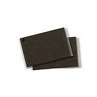
S29JL032H70TFI020 Spansion Inc., S29JL032H70TFI020 Datasheet - Page 34

S29JL032H70TFI020
Manufacturer Part Number
S29JL032H70TFI020
Description
IC,EEPROM,NOR FLASH,2MX16/4MX8,CMOS,TSSOP,48PIN,PLASTIC
Manufacturer
Spansion Inc.
Datasheets
1.S29JL032H70TFI020.pdf
(66 pages)
2.S29JL032H70TFI020.pdf
(66 pages)
3.S29JL032H70TFI020.pdf
(64 pages)
4.S29JL032H70TFI020.pdf
(66 pages)
Specifications of S29JL032H70TFI020
Data Bus Width
8 bit, 16 bit
Architecture
Boot Sector
Interface Type
Conventional
Access Time
70 ns
Supply Voltage (max)
3.6 V
Supply Voltage (min)
2.7 V
Maximum Operating Current
2 mA
Mounting Style
SMD/SMT
Memory Type
Flash
Memory Size
32 Mbit
Operating Temperature
+ 85 C
Package / Case
TSOP-48
Lead Free Status / RoHS Status
Lead free / RoHS Compliant
Lead Free Status / RoHS Status
Lead free / RoHS Compliant
Available stocks
Company
Part Number
Manufacturer
Quantity
Price
Company:
Part Number:
S29JL032H70TFI020H
Manufacturer:
SPANSION
Quantity:
30
34
Chip Erase Command Sequence
Chip erase is a six bus cycle operation. The chip erase command sequence is ini-
tiated by writing two unlock cycles, followed by a set-up command. Two
additional unlock write cycles are then followed by the chip erase command,
which in turn invokes the Embedded Erase algorithm. The device does not require
the system to preprogram prior to erase. The Embedded Erase algorithm auto-
matically preprograms and verifies the entire memory for an all zero data pattern
prior to electrical erase. The system is not required to provide any controls or tim-
ings during these operations. Table
for the chip erase command sequence.
When the Embedded Erase algorithm is complete, that bank returns to the read
mode and addresses are no longer latched. The system can determine the status
of the erase operation by using DQ7, DQ6, DQ2, or RY/BY#. Refer to the Write
Operation Status section for information on these status bits.
Any commands written during the chip erase operation are ignored. However,
note that a hardware reset immediately terminates the erase operation. If that
occurs, the chip erase command sequence should be reinitiated once that bank
has returned to reading array data, to ensure data integrity. Note that the SecSi
Sector, autoselect, and CFI functions are unavailable when an erase operation is
in progress.
Note: See Table
Increment Address
Figure 4. Program Operation
A D V A N C E
Embedded
in progress
13
algorithm
Program
for program command sequence.
S29JL032H
13
shows the address and data requirements
No
Command Sequence
I N F O R M A T I O N
Write Program
Last Address?
Programming
from System
Verify Data?
Completed
Data Poll
START
Yes
Yes
No
S29JL032HA0 May 21, 2004


