PIC24FJ16MC102-I/SS Microchip Technology, PIC24FJ16MC102-I/SS Datasheet - Page 145
PIC24FJ16MC102-I/SS
Manufacturer Part Number
PIC24FJ16MC102-I/SS
Description
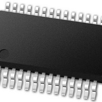
16-bit Motor Control Family, 16 MIPS, 16KB Flash, 1KB RAM 28 SSOP .209in TUBE
Manufacturer
Microchip Technology
Series
PIC® 24Fr
Datasheet
1.PIC24FJ16MC101-IP.pdf
(304 pages)
Specifications of PIC24FJ16MC102-I/SS
Processor Series
PIC24FJ
Core
PIC
Data Bus Width
16 bit
Program Memory Type
Flash
Program Memory Size
16 KB
Data Ram Size
1 KB
Maximum Operating Temperature
+ 85 C
Mounting Style
SMD/SMT
Package / Case
SSOP-28
Development Tools By Supplier
MPLAB IDE Software
Minimum Operating Temperature
- 40 C
Core Processor
PIC
Core Size
16-Bit
Speed
16 MIPs
Connectivity
I²C, IrDA, LIN, SPI, UART/USART
Peripherals
Brown-out Detect/Reset, Motor Control PWM, POR, PWM, WDT
Number Of I /o
21
Eeprom Size
-
Ram Size
1K x 8
Voltage - Supply (vcc/vdd)
3 V ~ 3.6 V
Data Converters
A/D 6x10b
Oscillator Type
Internal
Operating Temperature
-40°C ~ 85°C
Lead Free Status / Rohs Status
Details
Available stocks
Company
Part Number
Manufacturer
Quantity
Price

Part Number:
PIC24FJ16MC102-I/SS
Manufacturer:
MICROCHIP/微芯
Quantity:
20 000


REGISTER 15-6:
© 2011 Microchip Technology Inc.
bit 15
bit 7
Legend:
R = Readable bit
-n = Value at POR
bit 15-12
bit 11-8
bit 7-3
bit 2
bit 1
bit 0
U-0
U-0
—
—
Unimplemented: Read as ‘0’
SEVOPS<3:0>: PWM Special Event Trigger Output Postscale Select bits
1111 = 1:16 postscale
•
•
•
0001 = 1:2 postscale
0000 = 1:1 postscale
Unimplemented: Read as ‘0’
IUE: Immediate Update Enable bit
1 = Updates to the active PxDC registers are immediate
0 = Updates to the active PxDC registers are synchronized to the PWM time base
OSYNC: Output Override Synchronization bit
1 = Output overrides via the PxOVDCON register are synchronized to the PWM time base
0 = Output overrides via the PxOVDCON register occur on next T
UDIS: PWM Update Disable bit
1 = Updates from Duty Cycle and Period Buffer registers are disabled
0 = Updates from Duty Cycle and Period Buffer registers are enabled
U-0
U-0
—
—
PWMxCON2: PWM CONTROL REGISTER 2
‘1’ = Bit is set
W = Writable bit
U-0
U-0
—
—
U-0
U-0
Preliminary
—
—
U = Unimplemented bit, read as ‘0’
‘0’ = Bit is cleared
R/W-0
U-0
—
PIC24FJ16MC101/102
R/W-0
R/W-0
IUE
SEVOPS<3:0>
CY
boundary
x = Bit is unknown
OSYNC
R/W-0
R/W-0
DS39997B-page 145
R/W-0
R/W-0
UDIS
bit 8
bit 0
Related parts for PIC24FJ16MC102-I/SS
Image
Part Number
Description
Manufacturer
Datasheet
Request
R

Part Number:
Description:
Manufacturer:
Microchip Technology Inc.
Datasheet:
Part Number:
Description:
Manufacturer:
Microchip Technology Inc.
Datasheet:
Part Number:
Description:
Manufacturer:
Microchip Technology Inc.
Datasheet:
Part Number:
Description:
Manufacturer:
Microchip Technology Inc.
Datasheet:
Part Number:
Description:
Manufacturer:
Microchip Technology Inc.
Datasheet:
Part Number:
Description:
Manufacturer:
Microchip Technology Inc.
Datasheet:
Part Number:
Description:
Manufacturer:
Microchip Technology Inc.
Datasheet:
Part Number:
Description:
Manufacturer:
Microchip Technology Inc.
Datasheet: