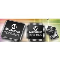
PIC18F44K22-I/MV Microchip Technology, PIC18F44K22-I/MV Datasheet - Page 152

PIC18F44K22-I/MV
Manufacturer Part Number
PIC18F44K22-I/MV
Description
16KB, Flash, 768bytes-RAM,8-bit Family,nanoWatt XLP 40 UQFN 5x5x0.5mm TUBE
Manufacturer
Microchip Technology
Series
PIC® XLP™ 18Fr
Specifications of PIC18F44K22-I/MV
Core Processor
PIC
Core Size
8-Bit
Speed
64MHz
Connectivity
I²C, SPI, UART/USART
Peripherals
Brown-out Detect/Reset, HLVD, POR, PWM, WDT
Number Of I /o
35
Program Memory Size
16KB (8K x 16)
Program Memory Type
FLASH
Eeprom Size
256 x 8
Ram Size
768 x 8
Voltage - Supply (vcc/vdd)
1.8 V ~ 5.5 V
Data Converters
A/D 30x10b
Oscillator Type
Internal
Operating Temperature
-40°C ~ 85°C
Package / Case
40-UFQFN Exposed Pad
Processor Series
PIC18F
Core
PIC
Data Bus Width
8 bit
Data Ram Size
768 B
Number Of Programmable I/os
36
Number Of Timers
1 x 8-bit, 3 x 16-bit
Operating Supply Voltage
1.8 V to 5.5 V
Mounting Style
SMD/SMT
Lead Free Status / RoHS Status
Lead free / RoHS Compliant
Lead Free Status / RoHS Status
Lead free / RoHS Compliant
- Current page: 152 of 496
- Download datasheet (5Mb)
PIC18(L)F2X/4XK22
REGISTER 10-2:
REGISTER 10-3:
DS41412D-page 152
bit 7
Legend:
R = Readable bit
‘1’ = Bit is set
-n/n = Value at POR and BOR/Value at all other Resets
bit 7-4
bit 3
bit 2-0
Note 1:
bit 7
Legend:
R = Readable bit
-n = Value at POR
bit 7-6
bit 5
bit 4
bit 3-0
U-0
U-0
—
—
2:
3:
Port is available as input only when MCLRE = 0.
Writes to PORTx are written to corresponding LATx register. Reads from PORTx register is return of I/O
pin values.
Available on PIC18(L)F4XK22 devices.
Unimplemented: Read as ‘0’
RE3: PORTE Input bit value
RE<2:0>: PORTE I/O bit values
Unimplemented: Read as ‘0’
ANSA5: RA5 Analog Select bit
1 = Digital input buffer disabled
0 = Digital input buffer enabled
Unimplemented: Read as ‘0’
ANSA<3:0>: RA<3:0> Analog Select bit
1 = Digital input buffer disabled
0 = Digital input buffer enabled
U-0
U-0
—
—
PORTE: PORTE REGISTER
ANSELA – PORTA ANALOG SELECT REGISTER
W = Writable bit
‘0’ = Bit is cleared
W = Writable bit
‘1’ = Bit is set
ANSA5
R/W-1
U-0
—
(1)
(2), (3)
U-0
U-0
Preliminary
—
—
U = Unimplemented bit, read as ‘0’
x = Bit is unknown
U = Unimplemented bit, read as ‘0’
‘0’ = Bit is cleared
R/W-u/x
ANSA3
RE3
R/W-1
(1)
RE2
R/W-u/x
ANSA2
R/W-1
(2), (3)
2010 Microchip Technology Inc.
x = Bit is unknown
RE1
R/W-u/x
ANSA1
R/W-1
(2), (3)
RE0
R/W-u/x
ANSA0
R/W-1
(2), (3)
bit 0
bit 0
Related parts for PIC18F44K22-I/MV
Image
Part Number
Description
Manufacturer
Datasheet
Request
R

Part Number:
Description:
Manufacturer:
Microchip Technology Inc.
Datasheet:

Part Number:
Description:
Manufacturer:
Microchip Technology Inc.
Datasheet:

Part Number:
Description:
Manufacturer:
Microchip Technology Inc.
Datasheet:

Part Number:
Description:
Manufacturer:
Microchip Technology Inc.
Datasheet:

Part Number:
Description:
Manufacturer:
Microchip Technology Inc.
Datasheet:

Part Number:
Description:
Manufacturer:
Microchip Technology Inc.
Datasheet:

Part Number:
Description:
Manufacturer:
Microchip Technology Inc.
Datasheet:

Part Number:
Description:
Manufacturer:
Microchip Technology Inc.
Datasheet:


