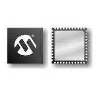
PIC16F1934-E/MV Microchip Technology, PIC16F1934-E/MV Datasheet - Page 12

PIC16F1934-E/MV
Manufacturer Part Number
PIC16F1934-E/MV
Description
7KB Flash, 256B RAM, 256B EEPROM, LCD, 1.8-5.5V 40 UQFN 5x5x0.5mm TUBE
Manufacturer
Microchip Technology
Series
PIC® XLP™ 16Fr
Datasheets
1.PIC16F722-ISS.pdf
(8 pages)
2.PIC16LF1933-ISS.pdf
(508 pages)
3.PIC16LF1933-ISS.pdf
(46 pages)
4.PIC16F1936-ISS.pdf
(2 pages)
5.PIC16F1936-ISS.pdf
(10 pages)
6.PIC16F1936-ISS.pdf
(40 pages)
7.PIC16F1936-ISS.pdf
(30 pages)
8.PIC16F1936-ISS.pdf
(12 pages)
Specifications of PIC16F1934-E/MV
Core Processor
PIC
Core Size
8-Bit
Speed
32MHz
Connectivity
I²C, LIN, SPI, UART/USART
Peripherals
Brown-out Detect/Reset, LCD, POR, PWM, WDT
Number Of I /o
36
Program Memory Size
7KB (4K x 14)
Program Memory Type
FLASH
Eeprom Size
256 x 8
Ram Size
256 x 8
Voltage - Supply (vcc/vdd)
1.8 V ~ 5.5 V
Data Converters
A/D 14x10b
Oscillator Type
Internal
Operating Temperature
-40°C ~ 125°C
Package / Case
40-UFQFN Exposed Pad
Processor Series
PIC16F
Core
PIC
Data Ram Size
256 B
Interface Type
MI2C, SPI, EUSART
Number Of Timers
5
Operating Supply Voltage
1.8 V to 5.5 V
Maximum Operating Temperature
+ 125 C
Mounting Style
SMD/SMT
Development Tools By Supplier
MPLAB IDE Software
Minimum Operating Temperature
- 40 C
Lead Free Status / RoHS Status
Lead free / RoHS Compliant
Lead Free Status / RoHS Status
Lead free / RoHS Compliant
PIC16F193X/LF193X
REGISTER 3-3:
DS41360A-page 12
bit 13
bit 6
Legend:
R = Readable bit
-n = Value at POR
bit 13
bit 12
bit 11
bit 10
bit 9
bit 8
bit 7-6
bit 5-4
bit 3-2
bit 1-0
Note 1:
R/P-1
LVP
U-1
2:
—
The LVP bit cannot be programmed to ‘0’ when Programming mode is entered via LVP.
Reads as ‘11’ on PIC16LF193X only.
LVP: Low-Voltage Programming Enable bit
1 = Low-voltage programming enabled
0 = HV on MCLR/V
DEBUG: In-Circuit Debugger Mode bit
1 = In-Circuit Debugger disabled, RB6/ICSPCLK and RB7/ICSPDAT are general purpose I/O pins
0 = In-Circuit Debugger enabled, RB6/ICSPCLK and RB7/ICSPDAT are dedicated to the debugger
Unimplemented: Read as ‘1’
BORV: Brown-out Reset Voltage Selection bit
1 = Brown-out Reset voltage set to 1.9V
0 = Brown-out Reset voltage set to 2.7V
STVREN: Stack Overflow/Underflow Reset Enable bit
1 = Stack overflow or underflow will cause a Reset
0 = Stack overflow or underflow will not cause a Reset
PLLEN: PLL Enable bit
1 = 4xPLL enabled
0 = 4xPLL disabled
Unimplemented: Read as ‘1’
VCAPEN<1:0>: Voltage Regulator Capacitor Enable bits
00 = V
01 = V
10 = V
11 = No capacitor on V
Unimplemented: Read as ‘1’
WRT<1:0>: Flash memory self-write protection bits
4 kW FLASH memory (PIC16F1933/PIC16LF1933 and PIC16F1934/PIC16LF1934 only):
8 kW FLASH memory (PIC16F1936/PIC16LF1936 and PIC16F1937/PIC16LF1937 only):
16 kW FLASH memory (PIC16F1938/PIC16LF1938 and PIC16F1939/PIC16LF1939 only):
VCAPEN1
DEBUG
11 = Write protection off
10 = 000h to 1FFh write protected, 200h to FFFh may be modified by EECON control
01 = 000h to 7FFh write protected, 800h to FFFh may be modified by EECON control
00 = 000h to FFFh write protected, no addresses may be modified by EECON control
11 = Write protection off
10 = 000h to 1FFh write protected, 200h to 1FFFh may be modified by EECON control
01 = 000h to FFFh write protected, 1000h to 1FFFh may be modified by EECON control
00 = 000h to 1FFFh write protected, no addresses may be modified by EECON control
11 = Write protection off
10 = 000h to 1FFh write protected, 200h to 3FFFh may be modified by EECON control
01 = 000h to 1FFFh write protected, 2000h to 3FFFh may be modified by EECON control
00 = 000h to 3FFFh write protected, no addresses may be modified by EECON control
CONFIGURATION WORD 2
R/P-1
R/P-1
CAP
CAP
CAP
functionality is enabled on RA0.
functionality is enabled on RA5.
functionality is enabled on RA6.
W = Writable bit
‘1’ = Bit is set
PP
VCAPEN0
must be used for programming.
CAP
R/P-1
U-1
—
pin.
Advance Information
(1)
BORV
R/P-1
U-1
—
(2)
U = Unimplemented bit, read as ‘0’
‘0’ = Bit is cleared
x = Bit is unknown
STVREN
R/P-1
U-1
—
© 2008 Microchip Technology Inc.
PLLEN
WRT1
R/P-1
R/P-1
WRT0
R/P-1
U-1
—
bit 7
bit 0


