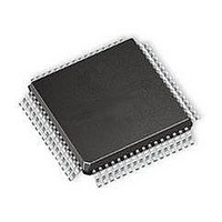
PIC16F1526-E/PT Microchip Technology, PIC16F1526-E/PT Datasheet - Page 167

PIC16F1526-E/PT
Manufacturer Part Number
PIC16F1526-E/PT
Description
64-pin, 14KB Flash, 768B RAM, 10-bit ADC, 10xCCP, 2xSPI, 2xMI2C, 2xEUSART, 2.3V-
Manufacturer
Microchip Technology
Series
PIC® XLP™ 16Fr
Datasheet
1.PIC16F1526-EMR.pdf
(354 pages)
Specifications of PIC16F1526-E/PT
Core Processor
PIC
Core Size
8-Bit
Speed
20MHz
Connectivity
I²C, LIN, SPI, UART/USART
Peripherals
Brown-out Detect/Reset, POR, PWM, WDT
Number Of I /o
54
Program Memory Size
14KB (8K x 14)
Program Memory Type
FLASH
Eeprom Size
-
Ram Size
768 x 8
Voltage - Supply (vcc/vdd)
2.3 V ~ 5.5 V
Data Converters
A/D 30x10b
Oscillator Type
Internal
Operating Temperature
-40°C ~ 125°C
Package / Case
64-TQFP
Processor Series
PIC16F
Core
PIC
Data Ram Size
768 B
Interface Type
MI2C, SPI, EUSART
Number Of Timers
9
Operating Supply Voltage
1.8 V to 5.5 V
Maximum Operating Temperature
+ 125 C
Mounting Style
SMD/SMT
Development Tools By Supplier
MPLAB IDE Software
Minimum Operating Temperature
- 40 C
Lead Free Status / Rohs Status
Lead free / RoHS Compliant
Available stocks
Company
Part Number
Manufacturer
Quantity
Price
Company:
Part Number:
PIC16F1526-E/PT
Manufacturer:
Microchip Technology
Quantity:
10 000
- Current page: 167 of 354
- Download datasheet (3Mb)
18.0
The Timer1/3/5 module is a 16-bit timer/counter with
the following features:
• 16-bit timer/counter register pair (TMRxH:TMRxL)
• Programmable internal or external clock source
• 2-bit prescaler
• Dedicated 32 kHz oscillator circuit
• Optionally synchronized comparator out
• Multiple Timer1/3/5 gate (count enable) sources
• Interrupt on overflow
• Wake-up on overflow (external clock,
• Time base for the Capture/Compare function
• Special Event Trigger (with CCP)
• Selectable Gate Source Polarity
FIGURE 18-1:
2011 Microchip Technology Inc.
Asynchronous mode only)
From Timer0
Overflow
Timer2/4/6
TxG
Overflow
Overflow
Timer10
TxGSS<1:0>
Note 1:
TIMER1/3/5 MODULE WITH
GATE CONTROL
(4)
2:
3:
4:
TxGPOL
ST Buffer is high-speed type when using TxCKI.
Timer1 register increments on rising edge.
Synchronize does not operate while in Sleep.
See
Set flag bit
TMRxIF on
Overflow
Table 18-4
00
10
11
TIMER1/3/5 BLOCK DIAGRAM
01
Secondary Oscillator
(See
TMRxON
TxGTM
for Timer selection.
TMRxH
Figure
TMRx
18-2)
TxG_IN
(2)
D
R
CK
TMRxL
Q
Q
Preliminary
TMRxCS<1:0>
SOSC/TxCKI
LFINTOSC
0
1
TxGGO/DONE
Q
Internal
Internal
F
OSC
Clock
Clock
F
OSC
EN
/4
D
• Gate Toggle mode
• Gate Single-pulse mode
• Gate Value Status
• Gate Event Interrupt
Figure 18-1
.
Single Pulse
Acq. Control
TxCLK
Note:
11
10
01
00
TxGSPM
PIC16(L)F1526/27
TxCKPS<1:0>
TxSYNC
Prescaler
1, 2, 4, 8
TMRxON
is a block diagram of the Timer1/3/5 module.
The ‘x’ variable used in this section is
used to designate Timer1, Timer3 or
Timer5. For example, TxCON references
T1CON, T3CON or T5CON. PRx refer-
ences PR1, PR3 or PR5.
0
1
2
0
1
Internal
F
Clock
TxGVAL
OSC
TMRxGE
/2
Q1
Synchronized
Synchronize
Interrupt
clock input
D
EN
det
det
Sleep input
Q
(3)
To Comparator Module
DS41458B-page 167
Set
TMRxGIF
T1GCON
Data Bus
RD
Related parts for PIC16F1526-E/PT
Image
Part Number
Description
Manufacturer
Datasheet
Request
R

Part Number:
Description:
IC, 8BIT MCU, PIC16F, 32MHZ, SOIC-18
Manufacturer:
Microchip Technology
Datasheet:

Part Number:
Description:
IC, 8BIT MCU, PIC16F, 32MHZ, SSOP-20
Manufacturer:
Microchip Technology
Datasheet:

Part Number:
Description:
IC, 8BIT MCU, PIC16F, 32MHZ, DIP-18
Manufacturer:
Microchip Technology
Datasheet:

Part Number:
Description:
IC, 8BIT MCU, PIC16F, 32MHZ, QFN-28
Manufacturer:
Microchip Technology
Datasheet:

Part Number:
Description:
IC, 8BIT MCU, PIC16F, 32MHZ, QFN-28
Manufacturer:
Microchip Technology
Datasheet:

Part Number:
Description:
IC, 8BIT MCU, PIC16F, 32MHZ, QFN-28
Manufacturer:
Microchip Technology
Datasheet:

Part Number:
Description:
IC, 8BIT MCU, PIC16F, 32MHZ, SSOP-20
Manufacturer:
Microchip Technology
Datasheet:

Part Number:
Description:
IC, 8BIT MCU, PIC16F, 20MHZ, DIP-40
Manufacturer:
Microchip Technology
Datasheet:

Part Number:
Description:
IC, 8BIT MCU, PIC16F, 32MHZ, QFN-28
Manufacturer:
Microchip Technology
Datasheet:

Part Number:
Description:
IC, 8BIT MCU, PIC16F, 20MHZ, MQFP-44
Manufacturer:
Microchip Technology
Datasheet:

Part Number:
Description:
IC, 8BIT MCU, PIC16F, 20MHZ, QFN-20
Manufacturer:
Microchip Technology
Datasheet:

Part Number:
Description:
IC, 8BIT MCU, PIC16F, 32MHZ, QFN-28
Manufacturer:
Microchip Technology
Datasheet:

Part Number:
Description:
MCU 14KB FLASH 768B RAM 64-TQFP
Manufacturer:
Microchip Technology
Datasheet:

Part Number:
Description:
7 KB Flash, 384 Bytes RAM, 32 MHz Int. Osc, 16 I/0, Enhanced Mid Range Core, Low
Manufacturer:
Microchip Technology

Part Number:
Description:
14KB Flash, 512B RAM, 256B EEPROM, LCD, 1.8-5.5V 40 UQFN 5x5x0.5mm TUBE
Manufacturer:
Microchip Technology
Datasheet:


