PIC16F1526-E/PT Microchip Technology, PIC16F1526-E/PT Datasheet - Page 133
PIC16F1526-E/PT
Manufacturer Part Number
PIC16F1526-E/PT
Description
64-pin, 14KB Flash, 768B RAM, 10-bit ADC, 10xCCP, 2xSPI, 2xMI2C, 2xEUSART, 2.3V-
Manufacturer
Microchip Technology
Series
PIC® XLP™ 16Fr
Datasheet
1.PIC16F1526-EMR.pdf
(354 pages)
Specifications of PIC16F1526-E/PT
Core Processor
PIC
Core Size
8-Bit
Speed
20MHz
Connectivity
I²C, LIN, SPI, UART/USART
Peripherals
Brown-out Detect/Reset, POR, PWM, WDT
Number Of I /o
54
Program Memory Size
14KB (8K x 14)
Program Memory Type
FLASH
Eeprom Size
-
Ram Size
768 x 8
Voltage - Supply (vcc/vdd)
2.3 V ~ 5.5 V
Data Converters
A/D 30x10b
Oscillator Type
Internal
Operating Temperature
-40°C ~ 125°C
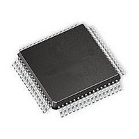
Package / Case
64-TQFP
Processor Series
PIC16F
Core
PIC
Data Ram Size
768 B
Interface Type
MI2C, SPI, EUSART
Number Of Timers
9
Operating Supply Voltage
1.8 V to 5.5 V
Maximum Operating Temperature
+ 125 C
Mounting Style
SMD/SMT
Development Tools By Supplier
MPLAB IDE Software
Minimum Operating Temperature
- 40 C
Lead Free Status / Rohs Status
Lead free / RoHS Compliant
Available stocks
Company
Part Number
Manufacturer
Quantity
Price
Company:

Part Number:
PIC16F1526-E/PT
Manufacturer:
Microchip Technology
Quantity:
10 000


REGISTER 12-22: ANSELE: PORTE ANALOG SELECT REGISTER
REGISTER 12-23: WPUE: WEAK PULL-UP PORTE REGISTER
TABLE 12-12: SUMMARY OF REGISTERS ASSOCIATED WITH PORTE
2011 Microchip Technology Inc.
bit 7
Legend:
R = Readable bit
u = Bit is unchanged
‘1’ = Bit is set
bit 7-3
bit 2-0
Note 1:
bit 7
Legend:
R = Readable bit
u = Bit is unchanged
‘1’ = Bit is set
bit 7-0
Note 1:
APFCON
ANSELE
LATE
PORTE
TRISE
WPUE
Legend:
R/W-1/1
WPUE7
Name
U-0
—
2:
When setting a pin to an analog input, the corresponding TRIS bit must be set to Input mode in order to
allow external control of the voltage on the pin.
Global WPUEN bit of the OPTION_REG register must be cleared for individual pull-ups to be enabled.
The weak pull-up device is automatically disabled if the pin is in configured as an output.
x = unknown, u = unchanged, - = unimplemented locations read as ‘ 0 ’. Shaded cells are not used by PORTE.
Unimplemented : Read as ‘ 0 ’
ANSE<2:0> : Analog Select between Analog or Digital Function on pins RE<2:0>, respectively
0 = Digital I/O. Pin is assigned to port or digital special function.
1 = Analog input. Pin is assigned as analog input
WPUE<7:0> : Weak Pull-up Register bits
1 = Pull-up enabled
0 = Pull-up disabled
TRISE7
WPUE7
LATE7
R/W-1/1
Bit 7
WPUE6
RE7
—
—
U-0
—
WPUE6
TRISE6
LATE6
Bit 6
RE6
W = Writable bit
x = Bit is unknown
‘0’ = Bit is cleared
W = Writable bit
x = Bit is unknown
‘0’ = Bit is cleared
—
—
R/W-1/1
WPUE5
U-0
—
TRISE5
WPUE5
LATE5
Bit 5
RE5
—
—
R/W-1/1
WPUE4
U-0
Preliminary
—
TRISE4
WPUE4
LATE4
Bit 4
RE4
—
—
U = Unimplemented bit, read as ‘0’
-n/n = Value at POR and BOR/Value at all other Resets
U = Unimplemented bit, read as ‘0’
-n/n = Value at POR and BOR/Value at all other Resets
R/W-1/1
WPUE3
WPUE3
TRISE3
LATE3
U-0
—
Bit 3
RE3
(1)
—
—
. Digital input buffer disabled.
PIC16(L)F1526/27
WPUE2
TRISE2
ANSE2
LATE2
Bit 2
R/W-1/1
WPUE2
RE2
ANSE2
R/W-1
—
T3CKISEL CCP2SEL
WPUE1
TRISE1
ANSE1
LATE1
Bit 1
RE1
R/W-1/1
ANSE1
WPUE1
R/W-1
TRISE0
WPUE0
ANSE0
LATE0
DS41458B-page 133
Bit 0
RE0
ANSE0
R/W-1/1
WPUE0
R/W-1
Register
on Page
124
133
132
132
132
133
bit 0
bit 0
Related parts for PIC16F1526-E/PT
Image
Part Number
Description
Manufacturer
Datasheet
Request
R

Part Number:
Description:
IC, 8BIT MCU, PIC16F, 32MHZ, SOIC-18
Manufacturer:
Microchip Technology
Datasheet:

Part Number:
Description:
IC, 8BIT MCU, PIC16F, 32MHZ, SSOP-20
Manufacturer:
Microchip Technology
Datasheet:

Part Number:
Description:
IC, 8BIT MCU, PIC16F, 32MHZ, DIP-18
Manufacturer:
Microchip Technology
Datasheet:

Part Number:
Description:
IC, 8BIT MCU, PIC16F, 32MHZ, QFN-28
Manufacturer:
Microchip Technology
Datasheet:

Part Number:
Description:
IC, 8BIT MCU, PIC16F, 32MHZ, QFN-28
Manufacturer:
Microchip Technology
Datasheet:
Part Number:
Description:
IC, 8BIT MCU, PIC16F, 32MHZ, QFN-28
Manufacturer:
Microchip Technology
Datasheet:
Part Number:
Description:
IC, 8BIT MCU, PIC16F, 32MHZ, SSOP-20
Manufacturer:
Microchip Technology
Datasheet:

Part Number:
Description:
IC, 8BIT MCU, PIC16F, 20MHZ, DIP-40
Manufacturer:
Microchip Technology
Datasheet:

Part Number:
Description:
IC, 8BIT MCU, PIC16F, 32MHZ, QFN-28
Manufacturer:
Microchip Technology
Datasheet:

Part Number:
Description:
IC, 8BIT MCU, PIC16F, 20MHZ, MQFP-44
Manufacturer:
Microchip Technology
Datasheet:

Part Number:
Description:
IC, 8BIT MCU, PIC16F, 20MHZ, QFN-20
Manufacturer:
Microchip Technology
Datasheet:
Part Number:
Description:
IC, 8BIT MCU, PIC16F, 32MHZ, QFN-28
Manufacturer:
Microchip Technology
Datasheet:

Part Number:
Description:
MCU 14KB FLASH 768B RAM 64-TQFP
Manufacturer:
Microchip Technology
Datasheet:
Part Number:
Description:
7 KB Flash, 384 Bytes RAM, 32 MHz Int. Osc, 16 I/0, Enhanced Mid Range Core, Low
Manufacturer:
Microchip Technology

Part Number:
Description:
14KB Flash, 512B RAM, 256B EEPROM, LCD, 1.8-5.5V 40 UQFN 5x5x0.5mm TUBE
Manufacturer:
Microchip Technology
Datasheet: