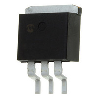
MCP1790-5002E/EB Microchip Technology, MCP1790-5002E/EB Datasheet - Page 6

MCP1790-5002E/EB
Manufacturer Part Number
MCP1790-5002E/EB
Description
High Voltage, LDO, 70 MA 3 DDPAK TUBE
Manufacturer
Microchip Technology
Datasheet
1.MCP1791T-3302EDC.pdf
(34 pages)
Specifications of MCP1790-5002E/EB
Regulator Topology
Positive Fixed
Voltage - Output
5V
Voltage - Input
6 ~ 30 V
Voltage - Dropout (typical)
0.7V @ 70mA
Number Of Regulators
1
Current - Output
70mA (Min)
Operating Temperature
-40°C ~ 125°C
Mounting Type
Surface Mount
Package / Case
TO-263-3, D²Pak (3 leads + Tab), TO-263AA
Number Of Outputs
1
Polarity
Positive
Input Voltage Max
30 V
Output Voltage
5 V
Output Type
Fixed
Dropout Voltage (max)
1.3 V at 70 mA
Output Current
70 mA
Line Regulation
+/- 0.0002 % / V
Load Regulation
+/- 0.2 %
Voltage Regulation Accuracy
2.5 %
Maximum Operating Temperature
+ 125 C
Mounting Style
SMD/SMT
Minimum Operating Temperature
- 40 C
Lead Free Status / RoHS Status
Lead free / RoHS Compliant
Current - Limit (min)
-
Lead Free Status / Rohs Status
Lead free / RoHS Compliant
Available stocks
Company
Part Number
Manufacturer
Quantity
Price
Company:
Part Number:
MCP1790-5002E/EB
Manufacturer:
MICROCHIP
Quantity:
50 210
MCP1790/MCP1791
AC/DC CHARACTERISTICS (CONTINUED)
DS22075A-page 6
Electrical Specifications: Unless otherwise noted, V
C
Boldface type applies for junction temperatures, T
Detect Threshold to PWRGD Active
Time Delay
AC Performance
Output Delay From SHDN
PWRGD Delay from SHDN
Output Noise
Power Supply Ripple Rejection Ratio
Thermal Shutdown Temperature
Thermal Shutdown Hysteresis
Short Circuit Recovery Time
Note 1:
OUT
= 4.7 µF (X7R Ceramic), C
2:
3:
4:
5:
6:
7:
8:
9:
The minimum V
V
Load regulation is measured at a constant junction temperature using low duty cycle pulse testing. Load regulation is
tested over a load range from 1 mA to the maximum specified output current.
The maximum allowable power dissipation is a function of ambient temperature, the maximum allowable junction
temperature and the thermal resistance from junction to air. (i.e., T
dissipation will cause the device operating junction temperature to exceed the maximum 165°C rating. Sustained
junction temperatures above 165°C can impact the device reliability.
The junction temperature is approximated by soaking the device under test at an ambient temperature equal to the
desired Junction temperature. The test time is small enough such that the rise in the Junction temperature over the
ambient temperature is not significant.
Dropout voltage is defined as the input-to-output voltage differential at which the output voltage drops 2% below its
nominal value that was measured with an input voltage of V
Sustained junction temperatures above 165°C can impact the device reliability.
The Short Circuit Recovery Time test is done by placing the device into a short circuit condition and then removing the
short circuit condition before the device die temperature reaches 125 °C. If the device goes into thermal shutdown, then
the Short Circuit Recovery Time will depend upon the thermal dissipation properties of the package and circuit board.
TCV
peraturerange. V
Parameters
R
is the nominal regulator output voltage.
OUT
= (V
OUT-HIGH
IN
OUT-LOW
, V
IN(MIN)
IN
- V
= 4.7 µF (X7R Ceramic), T
OUT-LOW
= lowest voltage measured over the temperature range.
must meet two conditions: V
TV
T
Symbol
SHDN_PG
t
DET-PWRG
PSRR
THERM
ΔT
T
T
e
) *10^6 / (V
D
OR
SD
N
SD
J
(Note 5) of -40°C to +125°C.
IN
= V
R
Min
* ΔTemperature), V
OUT(MAX)
—
—
—
—
—
—
—
—
—
—
A
= +25°C, SHDN > 2.4V.
IN
+ V
≥ 6.0V and V
Typ
235
200
400
157
1.2
IN
90
75
80
20
DROPOUT(MAX),
0
= V
R
A
OUT-HIGH
, T
+ V
J
, θ
IN
DROPOUT(MAX)
Max
—
—
—
—
—
—
—
—
—
—
JA
≥ V
). Exceeding the maximum allowable power
(Note 1), I
= highest voltage measured over the tem-
OUT(MAX)
µV/√Hz) I
Units
ms
dB
µs
µs
ns
°C
°C
© 2008 Microchip Technology Inc.
.
OUT
+ V
DROPOUT(MAX).
= 1 mA,
V
100 mV to V
100 mV
SHDN = GND to V
V
C
SHDN = V
C
V
I
V
f = 100 Hz
f = 1 kHz, V
f = 1 kHz, V
Rising Temperature
Falling Temperature
(Note 8)
OUT
OUT
OUT
OUT
IN
INAC
OUT
OUT
= 7.0V, C
= 50 mA, f = 1 kHz
= 10 mA,
= V
= GND to 95% V
= 1.0 µF
= 1.0 µF
= 400 mVpp
Conditions
PWRGD_TH
IN
R
R
PWRGD_TH
to GND
IN
= 5.0V
= < 5.0V
= 0 µF,
IN,
+
,
R,
-


