MCP1790-5002E/EB Microchip Technology, MCP1790-5002E/EB Datasheet - Page 13
MCP1790-5002E/EB
Manufacturer Part Number
MCP1790-5002E/EB
Description
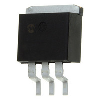
High Voltage, LDO, 70 MA 3 DDPAK TUBE
Manufacturer
Microchip Technology
Datasheet
1.MCP1791T-3302EDC.pdf
(34 pages)
Specifications of MCP1790-5002E/EB
Regulator Topology
Positive Fixed
Voltage - Output
5V
Voltage - Input
6 ~ 30 V
Voltage - Dropout (typical)
0.7V @ 70mA
Number Of Regulators
1
Current - Output
70mA (Min)
Operating Temperature
-40°C ~ 125°C
Mounting Type
Surface Mount
Package / Case
TO-263-3, D²Pak (3 leads + Tab), TO-263AA
Number Of Outputs
1
Polarity
Positive
Input Voltage Max
30 V
Output Voltage
5 V
Output Type
Fixed
Dropout Voltage (max)
1.3 V at 70 mA
Output Current
70 mA
Line Regulation
+/- 0.0002 % / V
Load Regulation
+/- 0.2 %
Voltage Regulation Accuracy
2.5 %
Maximum Operating Temperature
+ 125 C
Mounting Style
SMD/SMT
Minimum Operating Temperature
- 40 C
Lead Free Status / RoHS Status
Lead free / RoHS Compliant
Current - Limit (min)
-
Lead Free Status / Rohs Status
Lead free / RoHS Compliant
Available stocks
Company
Part Number
Manufacturer
Quantity
Price
Company:

Part Number:
MCP1790-5002E/EB
Manufacturer:
MICROCHIP
Quantity:
50 210


3.0
The descriptions of the pins are listed in
TABLE 3-1:
TABLE 3-2:
3.1
Connect the unregulated or regulated input voltage
source to V
eral inches away from the regulator or the input source
is a battery, it is recommended that an input capacitor
is used. A typical input capacitance value of 1 µF to
10 µF should be sufficient for most applications. The
type of capacitor used can be ceramic, tantalum or alu-
minum electrolytic. The low ESR characteristics of the
ceramic will yield better noise and PSRR performance
at high-frequency.
3.2
Tie GND to the negative side of the output and the
negative side of the input capacitor. Only the regulator
bias current flows out of this pin; there is no high
current. The regulator output regulation is referenced to
this pin. Minimize voltage drops between this pin and
the negative side of the load.
3.3
The V
ulator. A minimum output capacitance of 1.0 µF tanta-
lum, 1.0 µF electrolytic, or 4.7 µF ceramic is required
for stability. The MCP1790 is stable with ceramic,
tantalum, and electrolytic capacitors. See Section 4.7
“Output Capacitor” for output capacitor selection
guidance.
© 2008 Microchip Technology Inc.
SOT-223-3
SOT-223-5
Pin No.
Pin No.
2,Tab
Tab
—
OUT
1
3
1
2
3
4
5
PIN DESCRIPTIONS
Input Voltage Supply (V
Ground (GND)
Regulated Output Voltage (V
pin is the regulated output voltage of the reg-
IN
. If the input voltage source is located sev-
DDPAK-3
DDPAK-5
Pin No.
Pin No.
MCP1790 PIN FUNCTION TABLE
MCP1791 PIN FUNCTION TABLE
2,Tab
Tab
—
1
3
1
2
3
4
5
Symbol
PWRGD
Symbol
SHDN
V
GND
V
GND
V
N/C
V
OUT
OUT
—
IN
IN
IN
Table 3-1
)
Unregulated Supply Voltage
Ground Terminal
Regulated Output Voltage
Shutdown Input
Unregulated Supply Voltage
Ground Terminal
Regulated Output Voltage
Power Good Open-Drain Output
Connected to Ground
no connection
OUT
and
)
Table
3-2.
3.4
The SHDN pin is an active-low input signal that turns
the regulator output voltage on and off. When the
SHDN input is at a logic-high level, the regulator output
voltage is enabled. When the SHDN input is pulled to a
logic-low level, the regulator output voltage is disabled.
When the SHDN input is pulled low, the PWRGD output
signal also goes low and the regulator enters a low qui-
escent current shutdown state where the typical quies-
cent current is 10 µA. The SHDN pin is bonded to V
in the 3-pin versions of the regulator. See
3.5
The PWRGD pin is an open-drain output signal that is
used to indicate when the regulator output voltage is
within 90% (typically) of its nominal regulation value.
The PWRGD threshold has a typical hysteresis value
of 2%. The typical PWRGD delay time due to V
rising above 90% +3% (maximum hysteresis) is 30 µs.
The typical PWRGD delay time due to V
below 90% is 235 µs. These delay times are internally
fixed.
3.6
The DDPAK package has an exposed tab on the pack-
age. A heat sink may be mounted to the tab to aid in the
removal of heat from the package during operation.
The exposed tab or pad of all of the available packages
is at the ground potential of the regulator.
MCP1790/MCP1791
Shutdown (SHDN)
Power Good Output (PWRGD)
Exposed Pad (EP)
Function
Function
DS22075A-page 13
Table
OUT
4-1.
falling
OUT
IN
Related parts for MCP1790-5002E/EB
Image
Part Number
Description
Manufacturer
Datasheet
Request
R

Part Number:
Description:
High Voltage, LDO, 50 mA, -40C to +125C, 8-SOIC 150mil, TUBE
Manufacturer:
Microchip Technology
Datasheet:

Part Number:
Description:
IC LDO REG 70MA 5.0V SOT-223-3
Manufacturer:
Microchip Technology
Datasheet:

Part Number:
Description:
IC LDO REG 70MA 3.3V 3DDPAK
Manufacturer:
Microchip Technology
Datasheet:
Part Number:
Description:
IC LDO REG 70MA 3.0V SOT-223-3
Manufacturer:
Microchip Technology
Datasheet:
Part Number:
Description:
IC LDO REG 70MA 3.3V SOT-223-3
Manufacturer:
Microchip Technology
Datasheet:
Part Number:
Description:
IC LDO REG 70MA 3.0V 3DDPAK
Manufacturer:
Microchip Technology
Datasheet:

Part Number:
Description:
70 Ma, High Voltage Regulator
Manufacturer:
Microchip Technology Inc.
Datasheet:
Part Number:
Description:
Manufacturer:
Microchip Technology Inc.
Datasheet:
Part Number:
Description:
Manufacturer:
Microchip Technology Inc.
Datasheet:
Part Number:
Description:
Manufacturer:
Microchip Technology Inc.
Datasheet:
Part Number:
Description:
Manufacturer:
Microchip Technology Inc.
Datasheet:
Part Number:
Description:
Manufacturer:
Microchip Technology Inc.
Datasheet: