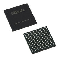
XC6SLX16-2FTG256C Xilinx Inc, XC6SLX16-2FTG256C Datasheet - Page 50

XC6SLX16-2FTG256C
Manufacturer Part Number
XC6SLX16-2FTG256C
Description
FPGA, SPARTAN-6 LX, 14K, 256FTGBGA
Manufacturer
Xilinx Inc
Series
Spartan® 6 LXr
Specifications of XC6SLX16-2FTG256C
No. Of Logic Blocks
2278
No. Of Macrocells
14579
Family Type
Spartan-6
No. Of Speed Grades
2
Total Ram Bits
589824
No. Of I/o's
186
Clock Management
DCM, PLL
I/o Supply Voltage
3.3V
Number Of Logic Elements/cells
14579
Number Of Labs/clbs
1139
Number Of I /o
186
Voltage - Supply
1.14 V ~ 1.26 V
Mounting Type
Surface Mount
Operating Temperature
0°C ~ 85°C
Package / Case
256-LBGA
Package
256FTBGA
Family Name
Spartan®-6
Device Logic Cells
14579
Device Logic Units
9112
Number Of Registers
18224
Typical Operating Supply Voltage
1.2 V
Maximum Number Of User I/os
186
Ram Bits
589824
Core Supply Voltage Range
1.14V
Rohs Compliant
Yes
Lead Free Status / RoHS Status
Lead free / RoHS Compliant
Number Of Gates
-
Lead Free Status / RoHS Status
Lead free / RoHS Compliant, Lead free / RoHS Compliant
Other names
122-1672
Available stocks
Company
Part Number
Manufacturer
Quantity
Price
Company:
Part Number:
XC6SLX16-2FTG256C
Manufacturer:
TI
Quantity:
21 500
Company:
Part Number:
XC6SLX16-2FTG256C
Manufacturer:
Xilinx Inc
Quantity:
10 000
DCM Switching Characteristics
Table 51: Operating Frequency Ranges and Conditions for the Delay-Locked Loop (DLL)
DS162 (v2.0) March 31, 2011
Preliminary Product Specification
Notes:
1.
2.
3.
4.
5.
Input Frequency Ranges
CLKIN_FREQ_DLL
Input Pulse Requirements
CLKIN_PULSE
Input Clock Jitter Tolerance and Delay Path Variation
CLKIN_CYC_JITT_DLL_LF
CLKIN_CYC_JITT_DLL_HF
CLKIN_PER_JITT_DLL
CLKFB_DELAY_VAR_EXT
DLL specifications apply when using any of the DLL outputs: CLK0, CLK90, CLK180, CLK270, CLK2X, CLK2X180, or CLKDV.
When operating independently of the DLL, the DFS supports lower CLKIN_FREQ_DLL frequencies. See
The CLKIN_DIVIDE_BY_2 attribute increases the effective input frequency range. When set to TRUE, the input clock frequency is divided by two as
it enters the DCM. Input clock frequencies for the clock buffer being used can be increased up to the F
BUFIO2 limits). When used with CLK_FEEDBACK=2X, the input clock frequency matches the frequency for CLK2X, and is limited to
CLKOUT_FREQ_2X.
CLKIN_FREQ_DLL input jitter beyond these limits can cause the DCM to lose LOCK, indicated by the LOCKED output deasserting. The user must
then reset the DCM.
When using both DCMs in a CMT, both DCMs must be LOCKED.
Symbol
Frequency of the CLKIN clock
Cycle-to-cycle jitter at the CLKIN
input when the CLKDV output is
not used.
Frequency of the CLKIN clock
input when using the CLKDV
output.
CLKIN pulse width as a
percentage of the CLKIN period
for
CLKIN_FREQ_DLL < 150 MHz
CLKIN pulse width as a
percentage of the CLKIN period
for
CLKIN_FREQ_DLL > 150 MHz
input for
CLKIN_FREQ_DLL < 150 MHz
Period jitter at the CLKIN input.
Allowable variation of the off-chip
feedback delay from the DCM
output to the CLKFB input.
Cycle-to-cycle jitter at the CLKIN
input for
CLKIN_FREQ_DLL > 150 MHz.
Description
(4)
www.xilinx.com
Spartan-6 FPGA Data Sheet: DC and Switching Characteristics
Min
5
5
40
45
–
–
–
–
(2)
(2)
-3
280
280
±300
±150
Max
60
55
±1
±1
(3)
(3)
Min
5
5
40
45
–
–
–
–
(2)
(2)
-3N
Speed Grade
280
280
±300
±150
Max
60
55
±1
±1
(3)
(3)
MAX
Table
(see
Min
5
5
40
45
–
–
–
–
(2)
(2)
Table 47
53.
-2
(1)
250
250
±300
±150
Max
60
55
±1
±1
(3)
(3)
and
Min
Table 48
5
5
40
45
–
–
–
–
(2)
(2)
-1L
175
133
±300
±150
Max
for BUFG and
60
55
±1
±1
(3)
(3)
Units
MHz
MHz
ps
ps
ns
ns
%
%
50


