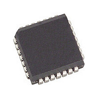
CY7B933-400JC Cypress Semiconductor Corp, CY7B933-400JC Datasheet - Page 8

CY7B933-400JC
Manufacturer Part Number
CY7B933-400JC
Description
Manufacturer
Cypress Semiconductor Corp
Datasheet
1.CY7B933-400JC.pdf
(33 pages)
Specifications of CY7B933-400JC
Lead Free Status / RoHS Status
Not Compliant
Available stocks
Company
Part Number
Manufacturer
Quantity
Price
Document #: 38-02017 Rev. *E
The Transmitter and Receiver parallel interface timing and
functionality can be made to match the timing and functionality
of either an asynchronous FIFO or a clocked FIFO by appro-
priately connecting signals (see Figure 4). Proper operation of
the FIFO interface depends upon various FIFO-specific
access and response specifications.
The HOTLink Transmitter and Receiver serial interface
provides a seamless interface to various types of media. A
minimal number of external components are needed to
properly terminate transmission lines and provide PECL loads.
For proper power supply decoupling, a single 0.01 µF for each
device is all that is required to bypass the V
Figure 5 illustrates a HOTLink Transmitter and Receiver
interface to fiber-optic and copper media. More information on
interfacing HOTLink to various media can be found in the
HOTLink Design Considerations application note.
CY7B923 HOTLink Transmitter Operating Mode
Description
In normal operation, the Transmitter can operate in either of
two modes. The Encoded mode allows a user to send and
receive eight-bit data and control information without first
converting it to transmission characters. The Bypass mode is
used for systems in which the encoding and decoding is
performed in an external protocol controller.
In either mode, data is loaded into the Input register of the
Transmitter on the rising edge of CKW. The input timing and
functional response of the Transmitter input can be made to
Q
SC/D,
RVS
CKR
RDY
0−7
RF
,
Q
SC/D,
RVS
DATA
RDY
CKR
0−7
INX
,
SERIAL DATA IN
FALLING EDGE OF CKR
±
RDY IS LOW FOR DATA
RF LATCHED ON
DATA
DATA
Figure 2. CY7B933 Receiver Data Pipeline in Encoded Mode
Figure 3. CY7B933 Framing Operation in Encoded Mode
RDY IS HIGH WHILE WAITING FOR K28.5
DATA
DATA
CC
RDY IS HIGH IN FIELD OF K28.5S
RECEIVER LATENCY= 24 t
and GND pins.
DATA
K28.5
DATA BOUNDARY CHANGES
CKR STRETCHES AS
match the timing and functionality of either an asynchronous
FIFO or a clocked FIFO by an appropriate connection of input
signals (see Figure 4). Proper operation of the FIFO interface
depends upon various FIFO-specific access and response
specifications.
Encoded Mode Operation
In Encoded mode the input data is interpreted as eight bits of
data (D
diagnostic input bit (SVS). If the context of the data is to be
normal message data, the SC/D input should be LOW, and the
data should be encoded using the valid data character set
described in the Valid Data Characters section of this
datasheet. If the context of the data is to be control or protocol
information, the SC/D input will be HIGH, and the data will be
encoded using the valid special character set described in the
Valid Special Character Codes and Sequences section.
Special characters include all protocol characters necessary
to encode packets for Fibre Channel, ESCON, proprietary
systems, and diagnostic purposes.
The diagnostic characters and sequences available as Special
Characters include those for Fibre Channel link testing, as well
as codes to be used for testing system response to link errors
and timing. A Violation symbol can be explicitly sent as part of
a user data packet (i.e., send C0.7; D
SC/D = 1), or it can be sent in response to an external system
using the SVS input. This will allow system diagnostic logic to
evaluate the errors in an unambiguous manner, and will not
require any modification to the transmission interface to force
transmission errors for testing purposes.
DATA
B
+ 10 ns
0
RDY IS LOW FOR LAST K28.5
–D
7
RDY IS LOW
), a context control bit (SC/D), and a system
FOR K28.5
K28.5
K28.5
DATA
RDY RESUMES
OPERATION
NORMAL
DATA
PARALLEL
DATA OUT
7–0
DATA
= 111 00000 and
CY7B923
CY7B933
Page 8 of 33


