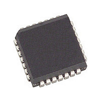
CY7B933-400JC Cypress Semiconductor Corp, CY7B933-400JC Datasheet - Page 26

CY7B933-400JC
Manufacturer Part Number
CY7B933-400JC
Description
Manufacturer
Cypress Semiconductor Corp
Datasheet
1.CY7B933-400JC.pdf
(33 pages)
Specifications of CY7B933-400JC
Lead Free Status / RoHS Status
Not Compliant
Available stocks
Company
Part Number
Manufacturer
Quantity
Price
Document #: 38-02017 Rev. *E
Maximum Ratings
(Above which the useful life may be impaired. For user guide-
lines, not tested.)
Storage Temperature ..................................–65°C to +150°C
Ambient Temperature with
Power Applied.............................................–55°C to +125°C
Supply Voltage to Ground Potential ............... –0.5V to +7.0V
DC Input Voltage............................................ –0.5V to +7.0V
Output Current into TTL Outputs (LOW) ......................30 mA
Output Current into PECL Outputs (HIGH) ................–50 mA
CY7B923/CY7B933 Electrical Characteristics
V
V
I
V
V
I
I
V
V
V
V
V
I
I
V
V
V
I
I
Notes:
10. Input currents are always positive at all voltages above V
Parameter
OST
IHT
ILT
IHE
ILE
IHH
ILL
7. See the last page of this specification for Group A subgroup testing information.
8. Tested one output at a time, output shorted for less than one second, less than 10% duty cycle.
9. Applies to A/B only.
TTL OUTs, CY7B923: RP; CY7B933: Q
TTL INs, CY7B923: D
Transmitter PECL-Compatible Output Pins: OUTA+, OUTA−, OUTB+, OUTB−, OUTC+, OUTC−
Receiver PECL-Compatible Input Pins: A/B, SI, INB
Differential Line Receiver Input Pins: INA+, INA−, INB+, INB−
OHT
OLT
IHT
ILT
OHE
OLE
ODIF
IHE
ILE
DIFF
IHH
ILL
[10]
[9]
[9]
Output HIGH Voltage
Output LOW Voltage
Output Short Circuit Current
Input HIGH Voltage
Input LOW Voltage
Input HIGH Current
Input LOW Current
Output HIGH Voltage
(V
Output LOW Voltage
(V
Output Differential Voltage
|(OUT+) − (OUT−)|
Input HIGH Voltage
Input LOW Voltage
Input HIGH Current
Input LOW Current
Input Differential Voltage
|(IN+) – (IN−)|
Highest Input HIGH Voltage
Lowest Input LOW Voltage
Input HIGH Current
Input LOW Current
CC
CC
referenced)
referenced)
0−7
Description
, SC/D, SVS, ENA, ENN, CKW, FOTO, BISTEN; CY7B933: RF, REFCLK, BISTEN
0−7
, SC/D, RVS, RDY, CKR, SO
I
I
V
V
V
Load = 50Ω to
V
Load = 50Ω to
V
Load = 50Ω to V
V
V
V
V
CC
OH
OL
CC
CC
OUT
IN
IN
IN
IN
IN
IN
/2.
= 4 mA
= - 2 mA
= V
= 0.0V
= V
= V
= V
= V
– 2V
– 2V
= 0V
CC
IHE
ILE
IHH
ILL
Min.
Min.
[8]
Max.
Max.
Over the Operating Range
Test Conditions
Com’l, Ind’l, and Mil
Ind’l and Mil (CKW and
FOTO, only)
Com’l
Ind’l and Mil
Com’l
Ind’l and Mil
Com’l
Ind’l and Mil
Com’l
Ind’l and Mil
CC
Static Discharge Voltage........................................... > 4001V
(per MIL-STD-883, Method 3015)
Latch-up Current..................................................... > 200 mA
Operating Range
Commercial
Industrial
– 2V
Range
[7]
–40
Temperature
0
°
Ambient
C to +70
V
°
V
V
V
V
V
C to +85
CC
CC
CC
CC
CC
CC
Min.
–0.5
+0.5
–200
–15
–10
2.4
2.0
2.2
0.6
2.0
2.0
2.0
– 1.165
50
– 1.03
– 1.05
– 1.86
– 1.96
– 1.14
°
C
°
C
V
V
V
V
V
V
CC
CC
CC
CC
CC
CC
Max.
–500
+500
CY7B923
CY7B933
0.45
V
V
V
V
V
–90
+10
750
0.8
– 1.475
– 0.83
– 0.83
– 1.62
– 1.62
– 1.50
CC
CC
CC
CC
CC
Page 26 of 33
5V ± 10%
5V ± 10%
V
CC
Unit
mA
mV
µA
µA
µA
µA
µA
µA
V
V
V
V
V
V
V
V
V
V
V
V
V
V
V
V


