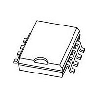
PCF8583T/F5,512 NXP Semiconductors, PCF8583T/F5,512 Datasheet - Page 16

PCF8583T/F5,512
Manufacturer Part Number
PCF8583T/F5,512
Description
Manufacturer
NXP Semiconductors
Datasheet
1.PCF8583TF5512.pdf
(28 pages)
Specifications of PCF8583T/F5,512
Bus Type
Serial (2-Wire, I2C)
Operating Supply Voltage (typ)
3.3/5V
Package Type
SO
Operating Supply Voltage (max)
6V
Operating Supply Voltage (min)
2.5V
Operating Temperature Classification
Industrial
Operating Temperature (max)
85C
Operating Temperature (min)
-40C
Pin Count
8
Mounting
Surface Mount
Date Format
DW:DM:M:Y
Time Format
HH:MM:SS:hh
Lead Free Status / RoHS Status
Not Compliant
Philips Semiconductors
9
9.1
Before any data is transmitted on the I
always carried out with the first byte transmitted after the start procedure.
The clock/calendar acts as a slave receiver or slave transmitter. Therefore the clock signal SCL is only an input signal,
but the data signal SDA is a bidirectional line.
The clock/calendar slave address is shown in Fig.16. Bit A0 corresponds to hardware address pin A0. Connecting this
pin to V
9.2
The I
1997 Jul 15
handbook, full pagewidth
Clock/calendar with 240
I
2
2
C-BUS PROTOCOL
C-bus configuration for the different PCF8583 READ and WRITE cycles is shown in Figs 17, 18 and 19.
Addressing
Clock/calendar READ/WRITE cycles
DD
or V
SS
allows the device to have one of two different addresses.
S
SLAVE ADDRESS
Fig.17 Master transmits to slave receiver (WRITE) mode.
handbook, halfpage
2
C-bus, the device which should respond is addressed first. The addressing is
acknowledgement
8-bit RAM
R/W
from slave
1
0 A
group 1
0
Fig.16 Slave address.
WORD ADDRESS
1
0
16
0
group 2
acknowledgement
0
from slave
A0 R/W
A
MRB016
n bytes
DATA
memory word address
auto increment
acknowledgement
from slave
A
MBD822
P
Product specification
PCF8583


